
Finishing up on the topic of CMOS bus logic I am going to show a couple of families with unique properties that may come in handy one day.
High Voltage Tolerant Family: AHC/AHCT
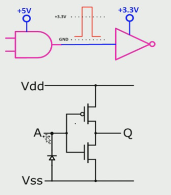
First up is a CMOS logic family AHC/AHCT that has one of the protection diodes on the input removed. This allows a 5V input voltage to be applied to a device powered by 3.3V so that I don’t have to add a gate just for the translation. Any time I can translate and do it without any additional gate delays I am a happy engineer.
Of course the example above works in a single direction and bidirectional does start to get more complicated. Using a bidirectional buffer such as a 74AHCT245 will work for TTL translation when going from 3.3V back to 5V providing there is a direction control signal present.
Dual Voltage Translating Transceiver
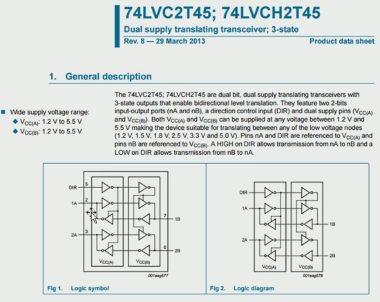 Another logic family by way of a true voltage translation is the dual supply translating transceiver, such as the 74LVC2T245. This part can translate from any voltage between 1.2-5.5V to any other voltage in that same range making it useful for the voltages below 2V up to TTL, and other combinations. This type device actually uses two power pins, one for each of the voltages being translated.
The 74LVC2T245 includes a “bus hold” function which can also be found in other logic families where they family name has an “H” in the name denoting the bus hold.
Bus Hold Function
The need for a bus hold function stems from the same concerns that makes us use lots of pull-up resistors; one for every single signal that has moments or possibilities of a high impedance tri-sate for any length of time, i.e. during a moment of tri-state where none of the possible bus drivers are turned on. This is a “floating” state where the voltage is free to wander around, unfortunately it can wander into the unspecified logic level state that is neither a logical high nor a low. Bad things happen at this point, current consumption goes way up (remember from last post when we talk about both transistors turning on at once between VCC and ground?) and things can actually oscillate, in fact you may not even see the oscillations with an oscilloscope as the oscillation could be occurring on the insides of chips attached to the bus.
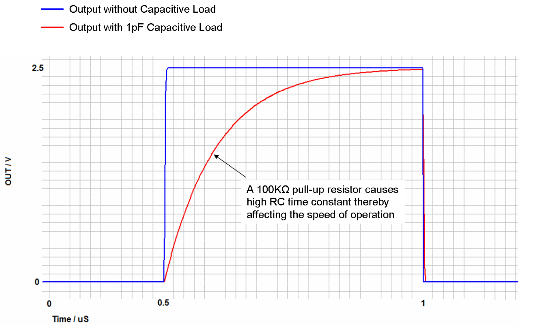
Weak pullups, meaning pull up resistors, can be added to all of the signals so that any signals left floating will eventually be pulled to a high state. There are several problems with pullups in general however; they add to the current consumption and the load on the bus and they can take a relatively long time to pull a voltage up into the “safe” high logic zone. By relatively long time I mean between 20-50ns or longer as a passive resistor suffers from an RC taper due to the inevitable capacitance found on a bus.
Making the pullup stronger, i.e. a smaller value, can have the undesired effect of more drastically increasing power consumption and reducing noise margin by “lifting“ the low voltage signals and making the buffers work harder when driving a low.
IC Chips and Dies
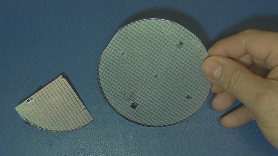
Switching gears I am going to talk a bit about the physical layout of integrated circuits. Shown is an old wafer I have left around from my time at Commodore in the 1980s. Looking under the microscope on my bench you can see the individual chip dies on the wafer. In production these would, after the appropriate testing and QA steps, be scribed and cut so that the individual dies can be mounted in individual chip packages.
If we zoom in further we can see some of what’s on the chip. Note that we are looking through a semi-transparent layer of insulation called passivation. At one time the chip designers could ask that a couple of wafers/dies skip the passivation step so that later they could better see and probe the chips under the microscope, though the lifetime of the chips was measured in months when exposed to the air without the protective passivation coating.


FET Side View
Showing a side view of how a Field Effect Transistor (FET) is made, the process starts by laying down an insulating layer and then masking a layer of polysilicon, a fairly conductive material that is used for the gate contact. It’s important to note that the gate will remain insulated from everything below it though there can be contacts upward to route to metal conductors and eventually to the pad and pins of the IC. The insulative layer can be seen under the gate in the drawing.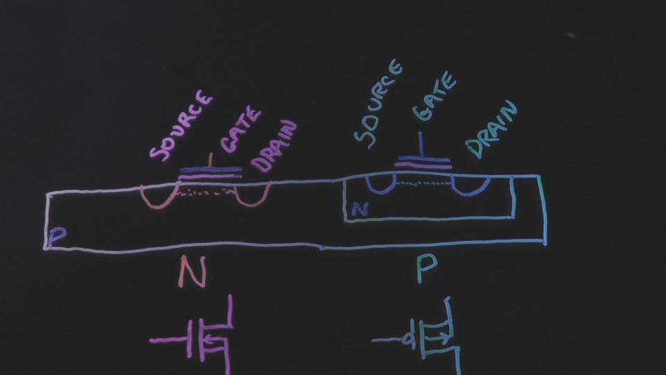
Once the gate is laid down the ends of what will be the transistor are then “implanted” by exposing the material to an ion implanter. We were always breaking our implanter back in the Commodore days as we were running ion densities higher than the implanter was designed for. This layer is called the diffusion layer harking back to a time when the layer was diffused via chemical doping.
The two diffusion zones now called the Source and Drain which are next to a polysilicon gate are what we need for the transistor to operate: apply the correct voltage to the gate and a conductive channel forms under the gate between the gate and source (shown in dotted lines above). Unlike a transistor which is bipolar, meaning it has a P and an N layer which are the makings of a diode (which conducts in only one direction), the FET supports current flow in either direction as the device is symmetrical, the drain and source are made of the same material with substrate between them.
![[Source: Wikipedia]](https://hackaday.com/wp-content/uploads/2015/09/cmos-side-view.png)
Speaking of substrate or the base layer that everything is grown on, it is either a N type or a P type. Most often it is a P-substrate these days which allows the N-channel devices to be grown directly on it, like NMOS technology did, the predecessor to CMOS. Before we can fabricate a P-channel transistor we have to first create a miniature version of some N-substrate that completely encompasses the area where the P-channel device will be. Looking at the diagram you will see the N-well which acts like an N-substrate. When CMOS first came out I remember reading about the pros and cons of using “dual tub” or both a P-well and N-well vs. just using a P-substrate, but I believe “single tub” or single well has won out, though there may be more parasitic considerations without the isolative properties of putting everything into a well (takes more room also!)
Now for the P-channel device, the same steps are basically the same once the N-well is implemented. When implanting, a different dopant is used to implant a P-diffusion drain and source than that used for N-diffusion. Examples of dopants are Boron for P+ diffusion and Arsenic for N+ diffusion.
Top View
Looking down from the top things look like a bunch of overlapping polygons, mostly because they are in fact a bunch of overlapping polygons. Most of the chip layout people I know have mentioned that they have dreamed about polygons in their sleep at some point.
If we look for the polysilicon and where it appears to overlap diffusion, though we know that it doesn’t really overlap as we saw in the side view, we can spot the transistors. The length of the channel underneath the polysilicon gate is where we get the “design rules” when talking about size, for example saying something is using 90nm rules means that the effective channel length between source and drain is 90 nanometers long.
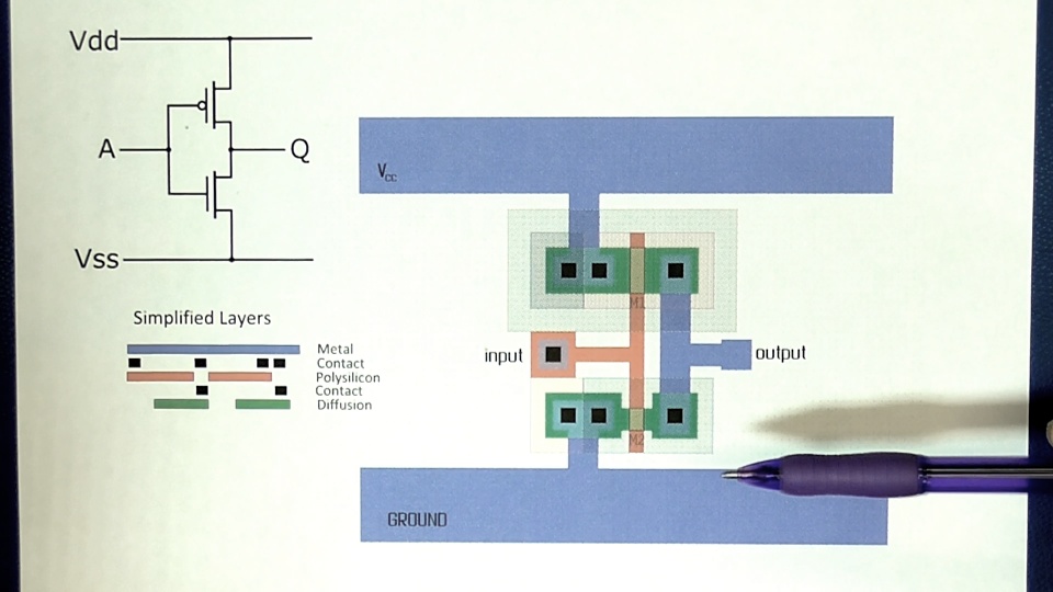
In the video I trace out the layout of the simple CMOS inverter as compared to the schematic.
Open Source “Magic” VLSI Editor
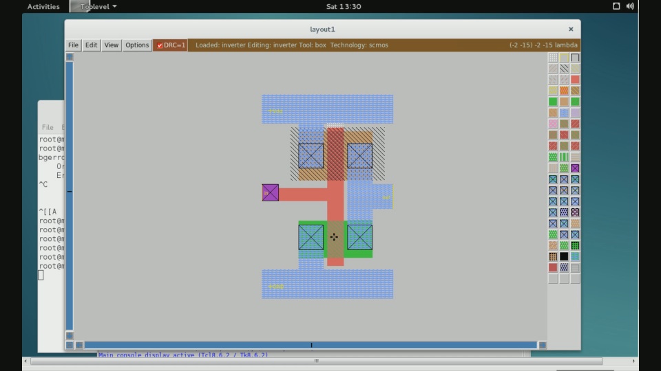
Lastly I wanted to show an open-source editing tool that allows us to play with some chip layout ourselves. The program is called Magic and its history and a download can be found here.
This is a great learning tool and design rule checks (DRC) built-in to the software can help someone first starting out in the craft to understand clearances and other rules regarding layout and production. The software can be hard to use at first: one must left click on a grid then right-click on the opposite corner of the desired polygon and then select the layer by middle clicking on the layer on the toolbar. Different rules can be loaded including scalable features and how a resistor or capacitor is made using various processes. Under the covers the DRC’s start kicking in and the various layers, masks and other photolithographic data can be extracted to start the process of going to chip fabrication.
But Why?
My style of engineering was always to look under the covers and I was fortunate to work at a couple of places where very smart people were there to explain to me what I was seeing or wanted to know. Understanding how ESD protection is implemented for example, can help an engineer understand what and what not may be a good design in various unusual circumstances where the datasheet alone doesn’t tell you everything.


Not too long. I’d watch these at 1/2 hour or hour lengths.
Interesting stuff! I’ve seen some pictures and videos of how they reverse-engineered the 6502 at visual6502.org and it looks all very intimidating but your video pretty much shows how to make out what each of those parts are.
And I agree, I’d definitely watch a longer video like this.
===Jac
Reminds me of this post,
http://hackaday.com/2015/01/28/resurrecting-capcoms-kabuki/
I can talk a lot longer! In fact its hard to shut me up. Maybe we can look at doing a supplemental video that’s not a heavily edited one.
I have exchanged emails with visual6502.org, great bunch. They have comments that are great given what I have been talking about, for example the things they look for that makes them assume that a FET is a Depletion type in special circuits. A lot can be learned from that site.
At Commodore we reverse engineered our main PLA, when you walked into the chip lab there was a big piece of cardboard with Polaroid pictures of a die stuck to it.
Yes please. I would love to watch hour-long video installments about this. There is so little info about how chips are actually made out there.
This talk has an incredible amount of detail on modern chip fabrication:
https://www.youtube.com/watch?v=NGFhc8R_uO4
I remember walking into the company we were using for layout once and finding a photomicrograph of the original BGA chip taking up most of the board room table, they’d hired a bunch of grad students for the summer to reverse engineer it (mostly by pattern matching gates rather than transistors) – not because thyey wanted to copy it but because they wanted to make a clone and everyone was worried at the time that there was hidden functionality that had not been released yet (in a sense there sort of was, if you didn’t get the datapath just right then unsupported stuff like ‘mode-X’ that Doom used wouldn’t work).
Now days this sort of reverse engineering is likely impracticable, both because chips are so much more complex these days, and also because multiple metal layers (rather than just 1 or 2) often with the top layer as a power plane hide the underlying gates
urgh that should be VGA chip
Yeah hugely complicated and dense though I believe some overseas companies are bootlegging jellybeans such as USB, one report was that there were three variations of the chip on the die (and still had problems).
We also had xray available, I remember we xrayed a few dongles including an early Orcad dongel to see what was in it.
There was a period (before 1990ish) when copyright did not extend to chip die, you could legally copy someone’s chip (and some did) just by optically recreating the masks from die photos. This resulted in people creating features on the die designed to fail when copied
My first job out of school was at Intel in 1987. Guess what the task was? Reverse engineer the new VGA chip from IBM that was part of their new PS/2 lineup. The MicroChannel architecture never took off, but VGA was quite successful. We used an array of about 80 poster sized die photos and some custom software that I wrote to keep track of all the cells and nets.
Luckily the old chips are “simple” compared to current tech and are fairly easy to reverse manually to preserve and study. And they’re a good source for learning how things were done. :)
image 1
and
image 2
Beware: Very memory consuming images!
Prior drawing these out I knew much of nothing about how FETs and such worked on the silicon level.
MOD EDIT: numbskull here embedded images that expand to 1.7GB. Made them links.
Dude, those huge images are crashing my chrome and opera browsers. Anyway, the images are awesome. I’m a sucker for high-res chip pictures. You could have posted only the links to the images though.
HaD guys, you should have some kind of image resolution/size checking before letting people post it in the comments section.
Woah. I didn’t realize those pictures were layout images. Which layout editor did you use to design them? Magic VLSI? I’m into chip design and layout myself and this is no small feat. Did you design them single-handedly?
Doesn’t look like the layout was drawn because the vias are round (they should be square). Was this layout image reverse engineered from the chip die picture using image processing somehow?
Both were done completely by hand in Photoshop over huge panoramic microscope photos of the dies requiring about two months per chip. Round vias are due to them appearing round on the die.
Looking at each chip revision it’s clear how the manufacturing process at MOS improved over time.
MODs: How about making the system to NOT embed images automatically, or have a toolbar of some sort giving options how to include links?
Magic gives me flashbacks to college. Saw polygons when I closed my eyes…
“Pushing polygons produces pretty pictures but begets blindness.”
We used MOSIS to fabricate the resulting chips which cost a few hundred dollars for a handful of small chips in the early 90s. Looks like they still exist:
https://www.mosis.com/
Wonder how much it cost for a shuttle run these days.
A friend [Harold Levy] ported Magic from BSD to Linux. One of the more annoying issues was that the BSD memory allocator allowed you to keep using free’d memory until the next allocation. Magic (ab)used this feature heavily, but linux doesn’t allow it. Good times!
Nowadays, an MPW (multi project wafer) shuttle for the latest tech node costs on the order of $100,000. This is a ballpark number. It varies based on many factors