As electronics engineer I have a mental collection of circuits that I’ve gathered over the years, much like a mechanic collects specialized tools as they work. All engineers do this and the tools in their tool boxes usually represent their project history and breadth.
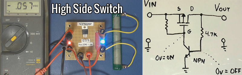
A useful circuit to have in designer’s toolbox is the “high side switch”. Like it sounds, this is a circuit that switches the “high side” or positive voltage to a load.
We usually tend to switch things to ground as seen by outputs such as an Open Collector output, the reason being that ground usually is a known entity and is usually low impedance and is at a known voltage. But there are advantages to using a high-side switch in your circuits.
Turning on the Voltage
Switching the high side deals with more unknowns than low side; the input voltage, the required output voltage, and the impedance of the source voltage are pretty much all variable. Most often we also need to present a low impedance output meaning that the resistance of the high side switch itself doesn’t form a voltage divider with the load where a significant voltage is dropped across the switch.

We could make a high side switch with a relay for example, and there are times when this is still done. Typically the properties of current usage, current capability, coil voltage, cost and size are at odds with each other.
If we use a standard transistor it’s a given that we are going to have to live with a voltage drop of some sort. On one end this means that we can’t have a 5 volt output from a 5 volt source as we typically lose 0.3v in the process. At high currents the power dissipation also quickly gets out of hand.
Enter the FET (again)
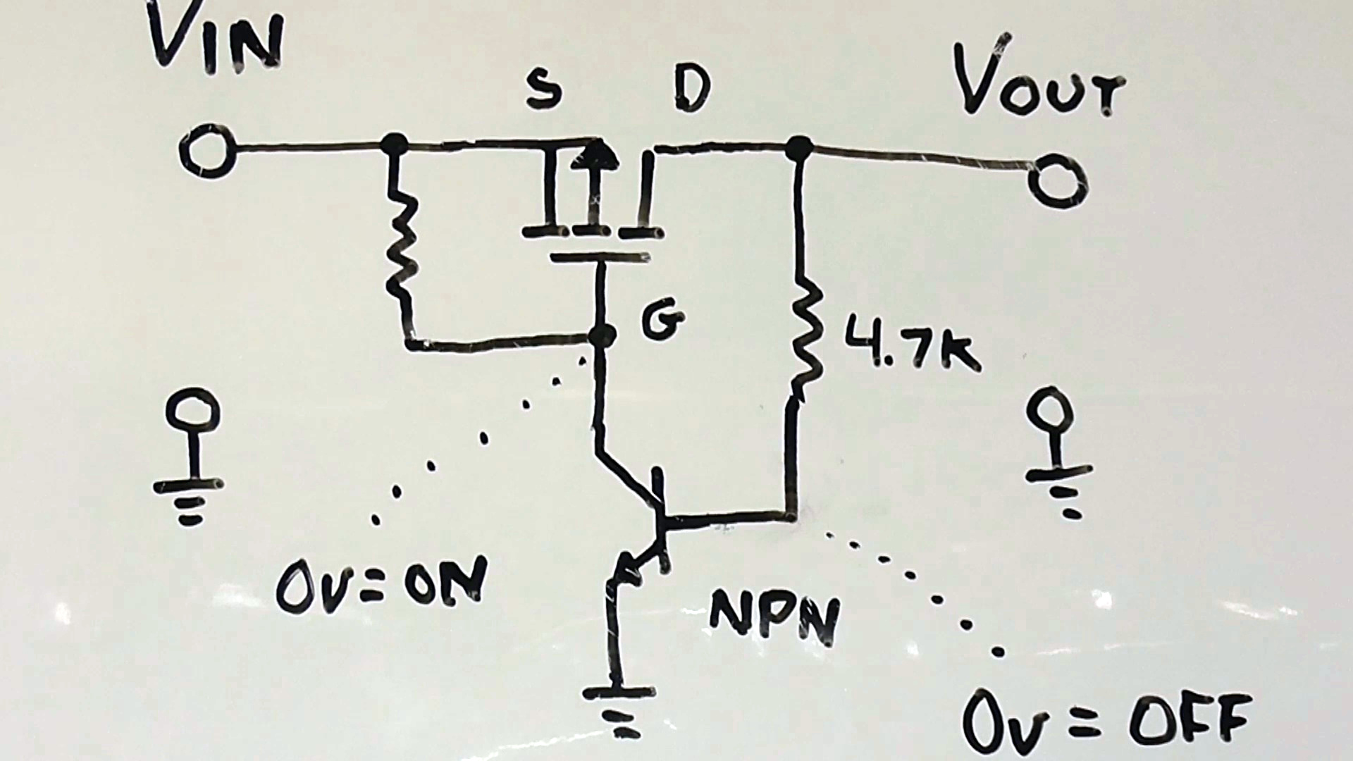
Using a Field Effect Transistor (FET) we can make use of some of its best qualities to make a switch. To narrow down on which FET we would use we can start by saying we want a part that normally is turned off and has to be turned on by applying a control voltage, meaning we want an Enhancement Mode FET. Next we decide whether we want to control the device by using a voltage greater than the voltage we are switching (if available) or less than the voltage. For example if we want to turn on 5 volts do we want to do that using 8 volts or more or 4 volts or less? In the example here we want to turn on the high side switch without an additional voltage, in fact grounding a signal is somewhat attractive. That leaves a P-Channel Enhancement FET as our choice.
The traits of any part can be wide and varied so we start by looking for a few important parameters. In switching applications, as opposed to something like a linear audio amplifier application, a low Drain to Source On Resistance is important. This parameter known as Resistance Drain to Source ON or RDS(ON) and a good usable part typically is measured in milliohms. Using ohms law a quick shortcut tells us that at one Amp of current, the voltage drop of milliohms will be millivolts.
Turning it on
Next we want to make sure that we can turn the part on with the voltage we have available. This equates to the Voltage Gate to Source Threshold VGS(thresh) specification. A VGS(thresh) of -1 v means that if we want to switch 3.3 volts we need to pull the gate at least 1 volt below 3.3 v. Using a transistor or open collector device typically can pull a signal within 0.3-0.5v of ground, plenty of room in this case to switch 2.5V using a part with a VGS(thresh) of a volt or so.
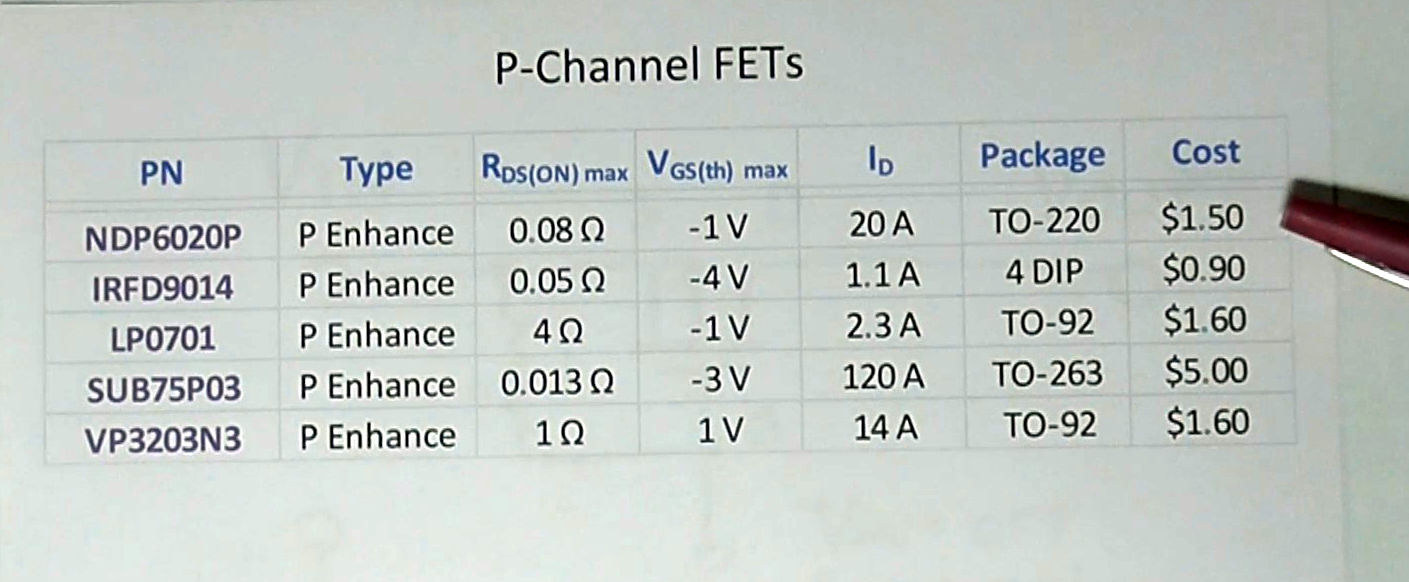
Looking at the specifications for several devices shown in the table, we see lots of trade-offs happening. If we select smaller TO-92 packages we get larger, unusable in our case, RDS(ON) values of an ohm or greater. If we go too small of an RDS(ON) the price quadruples. Other parts have too large of VGS(thresh) but the reality is it wasn’t too hard to find parts that were usable for the project shown here.
It’s About the Electrons, I Mean Holes
For those interested in peeking under the covers, the reason a larger case like a TO-220 has lower ON resistance is because the case holds a larger chip die. A larger chip die has a larger surface area which offers less resistance. The fact we are using a P Channel device means we need more surface area also, as P-Channel device are generally less efficient than N-Channel devices as they use “holes” for their carrier instead of electrons. The simplest statement is that hole mobility is less than electron mobility.
The switch circuit consists of two basic components, not counting add-on components that we would look at for a production worthy design such as reverse protection diode for the FET. With that said the FET shown does have a reverse avalanche diode built in for both overvoltage and reverse protection but it is the engineer’s job to determine if additional protection is needed.
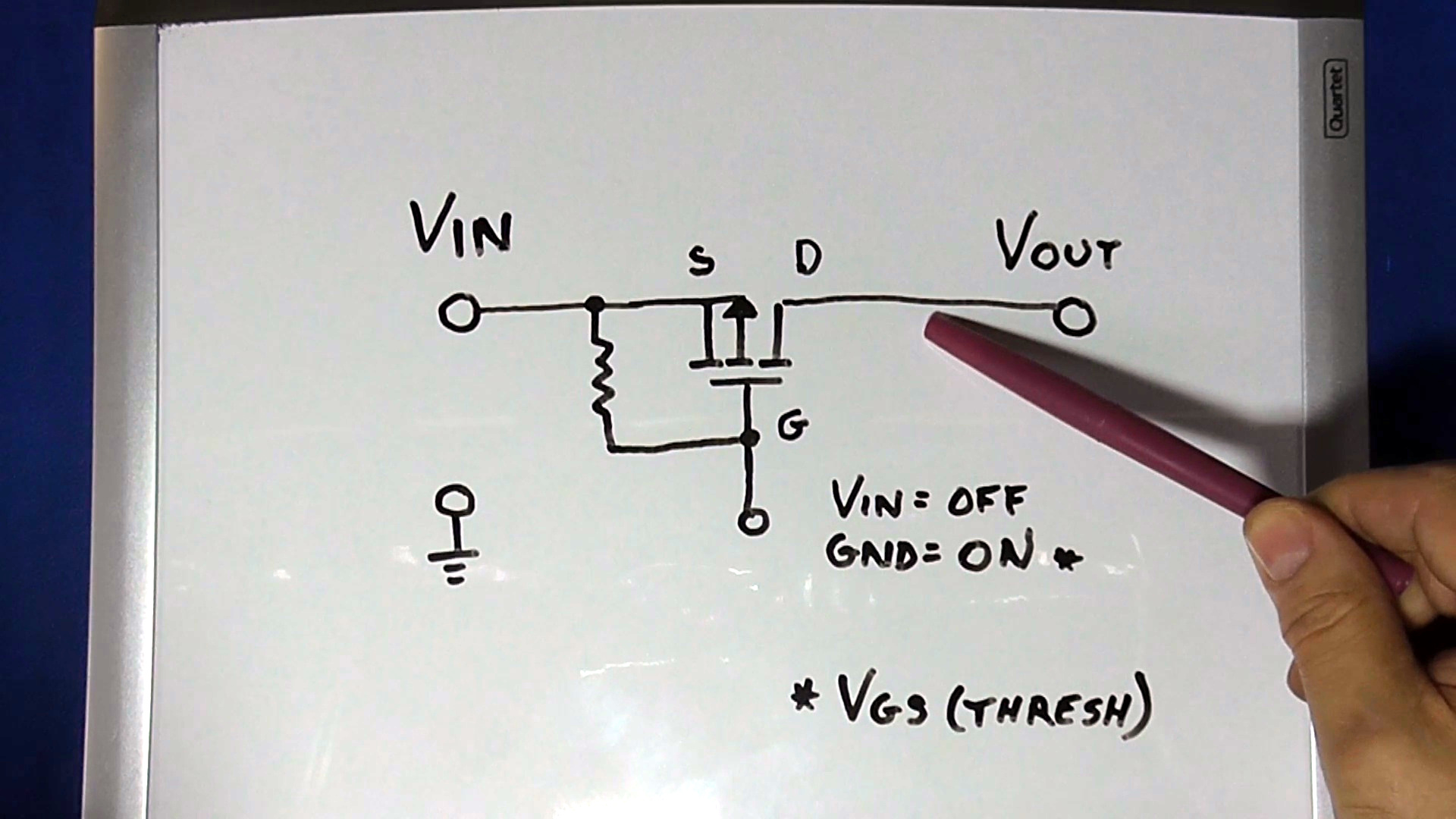
The resistor shown is a bias resistor and keeps the gate at a known value with no other input present, in this case it keeps the FET in the turned off or non-conductive state. In short the resistor keeps the FET in a VGS state of 0v when at least -1v is needed to turn it on.
Putting it to the Test
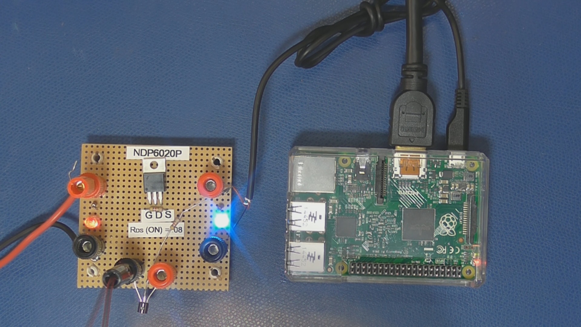
To demonstrate the effects of low RDS(ON) I have a circuit shown with a 5 Ohm load. Remembering Ohms Law and that E=IR, 5 Ohms load on 5 Volts yields a load current of 1 Amp. Using the same equation the RDS(ON) is easy to demonstrate using 1 Amp of current: A voltage drop of .057 volts at 1 Amp means that the resistance of the FET in this case is .057 Ohms! To put that in perspective for us, the power being dissipated by the device is P=I2R, or .057 watts or 57 milliwatts. We don’t really even have to do our thermal calculations to know that no heat sink is needed and that the device will work reliably used this way. To put it in perspective, the power dissipation of the load resistor is 5 watts, 87 times that of the switch itself.
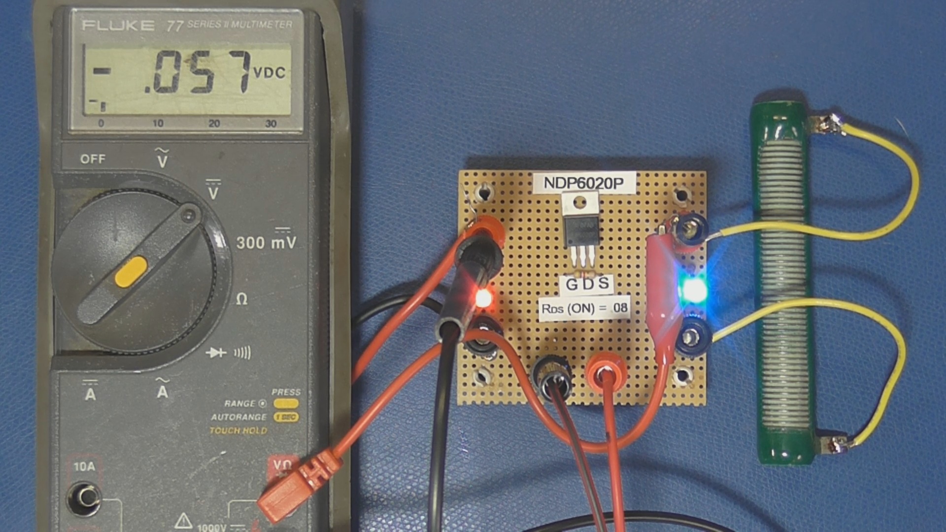
Since we only lose .057 volts in the process of turning on the load this means we can use a 5V supply as a source and still turn on a 5V load such as one of the many 5V controller or microcomputer boards available today…. this is almost as good as a mechanical switch.
Clap On, Clap Off
With the addition of a simple transistor and a resistor on its base to limit current, we can invert the signal needed to turn on the FET. This means we can create a push-on situation by having the load side voltage connect to the inverting transistor; once high the transistor will keep the FET turned on until something turns off the transistor.
My thoughts in showing a push-on circuit stems from thoughts about battery powered assemblies or applications where maybe a timer is used to turn off after a some amount of time. A controller based load can even turn off its own power supply, though this is a little more complicated where the load needs time to shut down cleanly such as a Linux based system, Raspbery PI for example.
Conclusion
Hopefully this is an example of a simple circuit which you may find useful at some point, at the very least we have explored the properties of a high side switch and a little bit about selecting a component by its specifications.


Nice lesson. Appreciated it.
+1
Something just as useful using the same principle, is the ideal diode in the Raspberry PI. It uses a high side switch like this, with a set of matched transistors to detect even the slightest differential in the voltage across the FET to turn it on or off.
…”But there are advantages to using a high-side switch in your circuits.”=?
(never explained) ;-)
Single part, no “higher” voltage or charge pump needed.
That only explains why you used a P-MOSFET as a high side switch, but not the the reason why a high side switch is useful.
Sometimes you want to keep the same Ground reference to your circuits, so switching the positive terminal with a high side switch.
Rob:
Thank you for the video BIll, but as you mentioned in the video the same circuit can be used for a N-channel low-side switch. Just flip everything. If you have a circuit with only a battery on the input, there’s no benefit to a high-side vs low-side. In fact, the low-side is better. If you need a common ground between the input power supply and another circuit, you’re better off with a high-side switch.
I like to use a ‘backwards’ N-channel then the N-channel version of this circuit on every battery project. The first N-channel provides an ideal diode, the second allows the circuit to turn itself off or allows me to add a switch to latch the battery on. It’s about as perfect a solution as you can get.
For me, the most important reason to use a high side switch has been that the common ground is always connected. Power supply -> MCU that controls the switch -> device being powered.
Try switching the power to a device with an MCU that also has other connections to the device being turned on. The switch has to be on the high side.
There are an awful lot of loads, including “hi voltage” that are turned on from MCU by low side switching. :)
but the issue is common grounds. say you turn the power off to a module using a low side switch, however one of its i/o pins is connected to a sensor that outputs a voltage, that power can backfeed through the protection diodes of the input and start to power the micro again, and if there’s any kind of significant load you risk damaging the pin.
got things mixed up, reverse it. ground is disconnected, sensor shorts to ground upon activation. backfeed occurs.
Ah, sensors (with more than just a power and ground pin) are one of the reasons I mentioned to use a high side switch. :)
One advantage to high side switching is safety. With a low side switch, even if it is switched off there is a possibility of an external ground causing current flow.
Lol… The previous home owner here had wired a switch on one of the wall outlets to control a plugged in lamp. When I went to work on it, since I trust nothing or anybody, I got my meter out and sure enough he had put the switch in series with the neutral and not the hot 110v. Great way to get knocked on one’s ass.
Safety? Couldn’t there then be a “possibility” of an “external high” causing current flow too then?
No. The “high” supplies power to the logic that controls the switch. Some other “external high” would then still be powering ON that logic which will then correctly control the switch. The danger with the low is that the switch could be activated while the logic that normally controls the switch is itself OFF.
You may want to switch a load on and off while maintaining a common ground with the load. Perhaps the load side has a sensor.
You may have a solder station and need to switch the heater on and off and maintain a ground for the temperature sensor.
You may have a current sense on the ground side so you need to switch on the high side.
Main reason for a high-side switch is where there is a common-ground path that can’t be avoided. Automotive circuits are a common example, where almost everything is grounded to the chassis, so switching the high-side is the only option.
Another example was a recent project I had where I was using a 5V LCD module with a 3.3V uC. The uC needed to be (nearly) always on, however it ran off battery so I had to turn off the LCD module except when needed. Although not plainly obvious, this was still a case where there was an unavoidable common ground.
If I was to use a simple low-side switch then when the LCD was off, there would still be a current path from the +5V of the LCD, through the data pins, through the in-built protection diodes in the uC, to the +3.3V rail, then through the 3.3V circuitry to ground. So there would constantly be current flowing through the LCD module. The only way to avoid this would be to buffer all the data lines between the LCD & the uC.
But with a high-side switch, and putting the uC outputs to logic 0, I could completely turn the device off with less components than would be needed for the buffering. Because the output of the uC wouldn’t be able to go high enough to completely turn off the driving transistor I had to use an additional open-collector NPN transistor in the gate with a pull-up resistor to pull the gate back to the supply voltage and turn it fully off.
If both my LCD module and uC were the same supply voltage, then low-side switching would have worked..
Another great video that went into my video “toolbox” for future reference. Casually tossing the RasPi, LOL
LOL, caught that did you. I tossed a 30 year old, one of a kind Commodore prototype into a bin in front of a room full of people, you could hear an audible hiss of many collectors as they drew breathe under duress.
“A voltage drop of .057 ohms at 1 Amp means that the resistance of the FET in this case is .057 Ohms!”
Should be
A voltage drop of .057 volts at 1 Amp means that the resistance of the FET in this case is .057 Ohms!
Corrected, thanks! I usually imply units when working and manually fill them in for public consumption which means I am bound to screw one up.
I have a problem in a circuit I am designing in that I need to switch a 24v rail with an N channel mosfet, using 3.3v
The design needs to be small and low cost. It’s switching upwards of 15A so I need to get the mosfet fully saturated. The problem is that the gate allows a maximum VGS of 20v, so most solutions I’ve found will not work. I researched into high side or low side IC Mosfet gate drivers, but it seems that most of them do not clamp the output voltage. 3.3v is too little, 24v is too much, and I don’t have room for a voltage regulator. High speed switching with a gate driver IC is preferred as it would reduce power losses. High-side or low-side doesn’t matter, high-side is preferred for safety reasons but most high-side drivers are ~2$ or they have a very large footprint (SOT323 or similar is my preference).
P-channel mosfets are seldom used in designs because of their efficiency and costs. I prefer N-channel.
I do this often – simply drive the gate with a resistor voltage divider – I.E. take his circuit and add a resistor between the gate and the transistor’s collector[or FET’s drain as the control element.] make sure the control transistor / FET can handle the 24V – when on, the resistor network limits how far “down” the gate is pulled.
this is a bad idea, it will affect switching times greatly. When dealing with 15 amps that can mean a LOT of power is lost.
To say “bad idea” is a bit harsh. It very much depends on the nature of the load and the duty cycle of the switching. In many cases a switching dissipation 1000 or 10000 times the average is no big deal. In many gross load situations (lamp, motor, heater…) a switching time going from microseconds to decimals of a second due to increased time constants makes no real difference provided the instantaneous ratings of the device(s) are not exceeded.
If you are driving some kind of switch mode power supply circuit then I would agree – keep the switching times short as you can.
Like all engineering…it depends on the situation as to what you can reasonably get away with.
I prefer N-Chan also. I would think that a low side gate driver would be be well limited in its vmax on its output based on its supply voltage or the charge pump technology it uses to boost voltage (I.E. dont power it from 24v) You didn’t say what the VDS(thresh) is for your part, if greater than 3.3v and that’s your only supply other than 24v then you may need a charge pump driven driver. The driver also deals with the capacitance needed for serious switching. If anything else can you switch out the FET for something more tolerant though honestly I double rate those things and 48v GS sounds like a lot on the surface.
All in all, your app sounds like a standard app for a MOSFET driver and I am surprised the exact right one doesn’t exist.
the charge pump drivers are $$$. The Vds on the part I’ve picked is 30V, but I’m assuming you mean Vgs, a max of +-20V, or the Vgs(th) threshold voltage of 1.95v MAX. The part is designed for 4.5V Gate voltage switching.
I picked a pretty hefty mosfet because there is only passive cooling and board space is limited. Though looking at it now, a 30V VDS might not be enough.
Have you tried looking into using optocouplers in your project? I’m using these a lot recently – I bought a big lot (1000) for a few cents pr. unit – as they satisfy most of my requirements for general switching, with the added benefit of isolating your MCU from things that can fry it.
Example circuit here: http://www.mikrocontroller.net/attachment/61816/opto.gif
A nice paper from Vishay about switching speeds: http://www.vishay.com/docs/83590/fastswit.pdf
The problem there is you loose other protections to the optocoupler/driver itself unless you also use a self protecting driver on your optocoupler output.
A part like ITS41K0SMEN provides current limiting and short protection which would just blow out an optocoupler with most of the benefits of a the optocoupler except that ground is now common. It would be really nice if there were an integrated optocoupler with protected outputs…
zener diode to limit the gate voltage (assuming you have a high enough value gate resistor)
Though you have to be careful that the gate resistor, if used, doesn’t form a big RC with the gate capacitance. At the least it has to be calculated/tested.
I did some simulations with this and using a 15v zener with a 220 ohm gate resistor yielded ok results, but the switch times will suffer, and the zener load is a bit over 0.5 watts which is quite a lot. I didn’t check how it would affect the gate switching times, but it kinda kills the added bonus of using a gate driver (most drive 2-5 Amps, this would limit it a lot).
I just thought of something, using a resistor+zener setup to feed the mosfet driver IC’s, instead of being on the gate. The mosfet drivers handle the surge current required to turn the mosfet on quickly (using a small cap as the source). when the gate is charged the current drops to near zero, so as long as switching is slow then the zener method would work without affecting switch-on times. Could add a cap in there too that will hold the charge after the gate drivers fire.
honestly it’s needlessly complex considering that the Vgs(max) for most mosfets is 20v, you’d think protection would be built-in.
a zener supple will work just fine with decoupling, the supply for the high side gate drive is already a capacitor, the boost capacitor.
Some fets have build in zener clamps on the gate
See TPS2816-2819: Gate driver + built-in regulator. Handles up to 40V supply and drive MOSFET with 10V.
Done.
I took a look at the TPS281x series, beautiful solution, however cost is huge. 2$ each is way above the price goal.
I found these: http://www.digikey.com/product-detail/en/MCP1402T-E%2FOT/MCP1402T-E%2FOTCT-ND/1956554
throw in a cheap LDO like this: http://www.digikey.com/product-detail/en/L78L15ABUTR/497-7769-1-ND/1883601
then it stays below budget concerns, and space concerns are not so big.
just use an integrated high side switch, something like auri3313 and a sot323 transistor and you have a high side switch with <10mOhm, +20A, thermal protection, short circuit protection, for few dollars
low side logic level N-channel? probably not going to do 15A in a SOT323 though…
google “smart high side switch” you will find some interesting ICs in typical transistor packages from a few manufacturers. They can normally be switched on with logic level and have different protections in them
MIC2505 has built in pass device and dual outputs for example.
There are gate drive with built-in regulator. e.g. TI TPS2816-2819 that can handle 40V input supply and regulate it to 10V for gate driving. It comes in a SOT23-5 and can handle 2A peak
A p-fet high side switch also makes a nice reverse polarity protection circuit.
On IC’s they actually/usually use FETS for the “diode” protection instead of real bipolar diodes.
great little latching push switch there. excellent. it’s always tempting to use micro’s and logic for some of these things, but that one is truly excellent. It’s almost like a simple SR flip flop! :)
Thanks It could have been done with a little N-Channel FET (look like a true SR) and also lower current for battery op but I went for something familiar so as to concentrate on the properties of the P-Chan.
EEVBlog (Dave Jones) did a very similar walkthrough a while back… https://www.youtube.com/watch?v=Foc9R0dC2iI
Reminds me of the Southpark episode where they keep saying “Simpsons Did It” , Probably true in this case with how long he has been doing it and how prolific Dave is. http://www.theamphour.com/222-an-interview-with-bil-herd-zany-z80-zygology/
Poor Butters.
Quote: “the reason a larger case like a TO-220 has lower ON resistance is because the case holds a larger chip die”
This is technically true, however you will find that with specifications that have been around for a while – that the TO-220 die would easily fit into the TO-92 case.
It simply may have been that the die was much larger when the semi was first manufactured and needed a larger case **at that time** and now it may fit easily into a smaller case but the **specification** remains with the larger case.
Even the early multi channel FET’s are on small dies now.
Now days the case style is more about the thermal characteristics of the specification than the die size.
PS: Great article [Bil Herd]
Great video, Bil! I always enjoy watching your videos, and this one made a subject that’s hard for new commers easy to understand – I know this, because I just sent it to a friend who had a “lightbulb above head”-moment after seeing it. Good job!
Great treatment of the subject, but a few notes, all of which I may have learned the hard way. I’ll use the NDP6020 as an example. As it’s a P FET, all the currents and voltages are negative, but many of the same principles hold for N FETs if you swap the sign
VGS(th) is generally specified at some nominal current, in this case, -250uA. -1V VGS will not fully turn on the FET. RDSon is rarely specified at VGS(th), generally at some lower value, in this case -2.5V.
Watch your VGS max. In the case of the NDP6020, if you try to switch 12V by pulling the gate to ground, you could blow up the FET. Worse, the gate junction could weaken over time and fail gradually or spectacularly at some point in the future.
When switching a FET, make sure the gate is well and truly at the source voltage when you want it off. Like, within tens of millivolts. Otherwise you will see some leakage and you will scratch your head. Gating 5V directly with a 3.3V GPIO and a P-FET won’t work, you’ll need a gate buffer transistor in there.
Agreed, in the video I mention that an engineer’s job is to check every spec also,at very high production qty’s missing a single spec can be a disaster. I did also briefly mention in the video the concept of turning the device all of the way on and off for the FET without really trying to get across just how freakin high of impedance the gate is (and yet still has a current spec) and I also didn’t talk about capacitance except maybe briefly.
Mentally picturing the thinness of the gate insulator and breakdown effects is a good placeholder for knowing some of the absolute max specs exist. Also I didn’t mention the fact that the transistor wouldn’t turn on without the bias resistor.
It’s weird how his head looks like it’s green-screened on the background, but then when the glasses are on his head later on you can see it isn’t. Has me wondering what causes that illusion.
Good video though.
Too often, but meaning nobody here so far, people convince themselves that they “need” a high-side switch because they don’t know very much and so can’t get their heads out of “switching the positive, high on and low off” (‘food good, fire bad”) lack of understanding.
Heh, kinda why I go on about holes and mobility as well as electrons to get down to the actual mechanisms where possible. I think most engineers I know go the opposite direction and look first at a switch to ground and work their way towards the need or something less common as needed.
I was pleased to find cheap, small, and high current FETs like the ao3400. It handles several amps in a sot23 package, has an on resistance of ~20 milliohms, and costs 2 cents in China.
http://www.aosmd.com
Digikey sells their parts too. Using their dual MOSFET in one project.
I used a low side switch in my mini laser cutter project and sure enough my choice was wrong. The switch was switching ground of the laser diode, but the package of diode was connected to ground terminal and thus it’s housing was grounded, which in turn was connected to laser cutters chassis, which was grounded. The result was that switch was bypassed and the laser was always on. Not very safe. I learned the use of high side switch the hard way. Thanks for the video tho :)
I like the high side integrated switches, like BTS4142N or the more powerful BTS441, for when you need smart stuff in your switch.
I had on my list of things to possibly talk about the real chips I would use for “real life” production that include short circuit sensing and a ton of other stuff. They are also engineered to create true Gate friendly drive signals.
“A voltage drop of .057 volts at 1 Amp means that the resistance of the FET in this case is .057 Ohms! To put that in perspective for us, the power being dissipated by the device is P=I2R, or .057 milliwatts.”
Actually, 0.057 Watts or 57 milliWatts. Great article though.
Fixed, thanks for pointing this out. I could have read it another 3 dozen times without catching that as I think I normalize the units in my retina before it ever hits the brain.
0v drop – use a knife switch, and then build a robot to open and close it based on a signal. You could just use a servo too, but that would lose the mad scientist factor. For extra credit, add a jacob’s ladder triggered by a tesla coil whenever the circuit is opened or closed. Sparky!
Thanks Bill, just what I needed as a solid-state relay for my motorcycle!
Thanks Bill.
I really need that info for some modifications on my sailng yacht.
Hans
Thank you for the elegant explanation. I want to drive a 5V laser with a 3.3V parallel port. I’d use low-side switching but for the common ground.
i had a problem of shorter time turn on of the P MOSFET while powered up with 50V even though both source and Gate are at same voltage of 50V
Thank you.I had a problem in switching 50V through P MOSFET. It gets turned on for shorter time when source and gate are powered with 50V. I can measure almost 25V at drain for shorter period even though both gate and source are at same potential.Please help me to get out of this problem
What is Vgs(max) for your fet? If you are trying to turn it on with 0V (as suggested in this article) and the Vgs(max) is less than 50V then you may have damaged your fet.
How do you size the bias resistor you connect between S and G. I understand that is is functioning basically as a pull-up, but have no idea what the value of it should be.
Hello!
i do not understand why i have only 90mA instead of about 337mA, any idea? thanks!
(see circuit on image)
https://drive.google.com/file/d/1MIk8UZWYRv3Dj_pGh2OsXzg_nAV-XUci/view?usp=sharing
Great insight on very simple high side switch! Thank you.
But you need to add two elements for stable operation.
first zenor for protect fet on high voltage and out put diode after TR output for protect capacitive load or this switch NOT off instaltly.
Also, I made and refined one button push on/off switch few yrs ago.
https://blog.naver.com/dgfiel/221501477883
Thanks for sharing information, I have question about using P channel mosfet for buck converter with simple gate driver , but I have problem that the Mosfet is always on? i can’t find the origin of this issue.