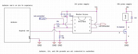
[Moser’s] introductory guide to MOSFETs serves as a quick introduction for those unfamiliar with the parts. They fill a similar role as a bipolar junction transistor like the 2N2222, making it possible to switch large loads. But fundamentally they are different. Metal Oxide Field Effect Transistors have three pins for Drain, Source, and Gate instead of the Collector, Emitter, and Base that you may be used to. The Gate is the control pin for the device and offers a desirable advantage over bipolar junction transistors in that it is insulated from the channel. This means that much less current flows into the Gate when compared to the Base of a common transistor, saving power and providing protection to the logic circuitry.
Don’t fret if this makes your head spin. [Moser’s] writeup is short and to-the-point but it’s not watered down. You can get a basic overview and if you care to learn more, he’s linked to datasheets and has basic terminology that is easily clarified with a Google search. One of the most powerful tools that he’s included is the simple MOSFET and driver circuit diagram you see above. This makes it possible to switch incredibly large loads very quickly; the true power of the MOSFET.


Use “logic level” MOSFETs and avoid the need for a driver…
Switching speed can still be an issue with larger transistors. However that’s quite a bit of ringing on his example using a driver.
DanJ is right. For large(r) MOSFETS one needs driving (turn on/off) gate current in amps to ensure fast “action”.
Direct impact of a slow turn on/off time is disipation (heat) – only when MOSFET is fully closed or opened, disipation is small, in “alinear” state it can be VERY significant.
Just a quick example, switching MOSFET conducting 10A of current. Typical Rds=0.01 ohm (Uds=0.1V) ==> power disipation = P = I^2*R = 1W
Somewhere in the linear state, just a guess, Id=8V, Uds=5V, Pd=40W. Can be even worst.
This also shows advantage of using MOSFET vs. bipolar – when “wide open”, voltage on MOSFET is only dependant on the current and Rds (not so rare to find NOSFETS with couple of miliomhs), while bipolar can’t go under Vcesat (saturation voltage), for large transistors in 1-2 volts range, so disipation for above imaginary example with a low Rds MOSFET (Rds=2mohm):
Pmosfet=Id*Uds=Id*Id*Rds=10A*10A*0.002 ohm=0.2W
Pbipolar=Ic*Ucesat=10A*2V=20W
http://www.falstad.com/circuit/#%24+1+5.0E-6+10.20027730826997+50+5.0+50f+432+256+480+256+0+1.5w+480+240+480+192+1172+480+192+480+160+0+6+5.0+5.0+0.0+0.0+0.5+Drain+Voltage162+480+320+480+384+1+2.1024259+1.0+0.0+0.0g+480+384+480+416+0r+480+272+480+320+0+100.0R+400+256+320+256+0+2+40.0+5.0+0.0+0.0+0.5w+400+256+432+256+0o+0+64+0+35+20.0+0.1+0+-1
sorry for the long link. Just came upon this site yesterday. thought it would be nice to share.
Why is is that any beginner that poorly and wrongly understands some concepts writes a tutorial? Please, correct the mistakes and stop making affirmations like: “MOSFET may need 10-15 Gate-Source potential difference”.
Here’s my constructive criticism: go learn about MOS transistors and when you understand them very well, then write a tutorial. There are plenty of books that cover the basic stuff, even online resources.
to HAD: please stop posting poor quality tutorials.
This ^^.
Surely you’re not that starved for content?
Realistically, you just have to be able to sink or source enough charge quickly to the gate of the mosfet. From a purely physics based model, you are driving a capacitive load(the gate of the mosfet). You should be able to use just a standard BJT or a lower gate capacitance mosfet as a single transistor mosfet driver. Doing that, you can sink or source the small amount of charge pretty quickly, without the cost of a driver!
And as DanJ pointed out… there is a significant amount of ringing. Yay for oscillators(glad he is just using it for switching, not analog signals!)
Now I’m waiting to see a decent write up on JFETs! ;)
the_truth, what you are saying, actually does not work (the part with a single BJT or other transistor as a driver). With a single active component you can either do a good job sinking or sourcing, not both, as the “other side” of your circuit (the other side of the half bridge) would end up being a resistor.
Using a half bridge circuit (two transistors on top of each other, when one open, the other closed) would do the job, but then you need some carfull design to prevent them form being open at the same time, plus sume other “minor” nuances. And you need those transistors to be able to deliver current in amps.
That’s where drivers rule, and usually end up being cheaper and more reliable solution.
That’s
In regards to the “ringing” that some posters mentioned (see the rising and falling edge), I can only guess that it’s a result of the long wiring to power supply.
When it comes to nano seconds, especially with “significant” currents (Ig might go above 1Amp easily), every wire twist counts.
Well in part, the trace/lead is the cause of the ringing. The trace/lead has a bit of inductance plus the gate being a capacitor gives you an LC oscillator. Just add a resistor to dampen and the ringing will be reduced. I want to say 100 ohms? but don’t quote me on the value.
btw saw these the other day, almost plug and play.
It has opto isolation for safety, and lots of current to turn on the gate of power mosfets.
http://www.mouser.com/avagoigbtoptocouplers/?cm_sp=homepage-_-newproducts-_-Avago+Technologies+IGBT+Gate+Drive+Optocouplers
You don’t have do do fast switching every time, if you are driving something, that you switch on-off a few times a minute, I suggest you don’t do fast switching especially with inductive loads – this can cause huge voltage spikes and EMI. When it comes to driving motors with PWM, it is something different.
And about the drivers, you don’t need them, look at all the RC brushless motor controllers – hardly any uses the driver. I was always considering the driver only for IGBT.