[Semicolo] has a bunch of old PSUs on hand which he pulled out of some Lexmark dot matrix printers. In their stock form they put out 40V, which is close to the 35V max he needs to run the stepper motors on a 3D printer he’s been building. So he reverse engineered the PSU to change its output.
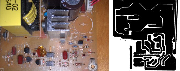
On the left you can see the top of the PCB. [Semicolo] flipped it over and snapped a picture of the traces on the bottom of the board. With a bit of work in The Gimp (FOSS image editing software) he was able to convert the traces to black and white. Overlaying the picture of the top with a 50% transparency of the traces made it rather easy see the connections and generate a schematic for the hardware. That’s a really cool trick!
Figuring out how it’s supposed to work is a big step in achieving his goal. The next step was to see if he could bend the circuit to his will. He had previously run across ATX PSU hacks which changed the reference voltage in order to alter the output. He grabbed a datasheet for the HA17431 variable shunt regulator. It lays out how to tune the output based on values of a few external components. He dropped in one resistor and the output measured 31V, well within his target range.


Now this IS a hack. Awesome idea with the transparency
Sure beats the run of the mill ATX PSU bench supply hacks I’m so sick of seeing.
Nice idea about components side pic + traces overlay. I agree that the schematic made from it makes the problem solving rather obvious, so well worth the effort.
I tried something like this a while back trying to troubleshoot an industrial controller whose maker has gone out of business (bought and sold many times and then absorbed and discontinued). The major problem I ran into was one of the daughterboards was a 8-layer nightmare with lots of tiny traces. The mainboard was relatively simple as it was just 2 layers with 1 of them being mainly a ground plane with LM317s, a transformer, and a PROM. This process really helped with that because I found out one of the traces between the layers burned open. Since the board was black in color it was hardly noticeable.
LM317s are linear regulators. The PSU in this article is obviously a switch mode power supply. So while they both regulate voltage the similarities stop there.
Think Josh is referring to the diagnostic techniques employed with regards to similarities.
I thought about that but considered the difference outweighed the similarities enough that I’d post anyways. There are several reasons SMPS are overwhelmingly fixed regulators. Where the LM317 is billed as a 3-Terminal Adjustable Regulator.
I probably could have been a bit clearer on that. I was actually talking about the diagnostic techniques. There was a PROM on the board and the traces ran from that to the daughterboard to a processor. The traces ran from that daughterboard to the main board to another daughterboard with isolation and digitally selected resistor circuitry then back to the LM317 to vary the voltage depending on what kind of output was needed.
There’s a reason the manufacturer went out of business. They made weird, overly complicated controllers and sold them for almost no profit margin hoping that they’d be able to get the repair business when the warranty expired because no one could figure out how they worked.
Seriously? Hell of a business plan. Almost as good as the one where you sell terrible software, forcing users to “upgrade” to the next version to fix all the bugs in the current one. An upgrade that comes with bugs of it’s own…
Capitalism, eh?
Et tu, Microsoft?
LM317 ICs themselves have only 3 pins and are almost as simple as it gets. They are straightforward devices even with digital adjustment schemes. Once it was discovered the design was so poor of the controller you were fixing the wise business decision would have been to replace it I suppose.
The maker went out of business before I got my hands on the controller or I would have just gotten another. It had 5 separate channels and you could change frequency and voltage for each channel from a touchscreen. It even had a 24/7 clock so you could control which channels came on and for how long. It was very fancy for what most people need and in a small cabinet. After finding the burnt trace, I ended up changing to a different controller with a larger cabinet with more reliability and ease of replacement.
No, it was pretty clear what you were posting about and your post was fine. ‘PCF11’ seems to have issues. It’s all about the method really, not the goal, and your method was similar.
Issues? Care to elaborate?
Well done! I often find myself with a power supply that is *close* to what I need. Having this info will certainly prove useful.
I have actually done this a lot, i have done a lot of things that require the standard 5V and 12V, but i had a lot of supplies that were somewhere close to that like 4.4V, 6.5V, 16V, 19V etc. that could be altered by changing the feedback voltage divider resistors.
The problems arise when you realize that some supplies regulate fine with a load but if you go below a couple of hundred mA the output voltage goes up a bit or starts to oscillate.
My point is: If you want to do a hack like this make sure you have an oscilloscope on hand to check that the output voltage is good at the new setting. It might look good on your multimeter but a scope will tell you if you have regulation problems, especially at low loads.
This is why I always add a power resistor across the output of my hacked switching supplies. It’s a bit wasteful, but the supply always sees enough load to prevent problems.
I do embedded systems engineering for a living. The comment about using a scope is spot-on. I *always* put a scope on the power whenever I bring up a board. Also, when the system starts acting weird – often it’s because the power glitches and it isn’t obviously the power is the root cause.
A meter has an integrator or low-pass filter so the input gets averaged. Last gig I was on, the (fairly new) EE was having problems. His cube was across from mine && I could hear the rant. I took a scope and hooked it to the power – it was obvious. Sometimes you need to impress the young bucks so they will listen to you later :^) He is going to make a *great* EE.
I do like the method. Easier than keep flipping the board.
I’ve done this a few times:
1) Connect a voltmeter to the output.
2) Connect a 100K resistor to a spare set of multimeter probes. Value chosen this high so you can get away with briefly connecting it to the wrong things.
3) With the supply powered, *carefully* try briefly bridging each likely resistor in it, in turn, with the probes. Record any that cause a small change in output voltage, by how much, and in which direction.
When done, you’ll have a pretty good idea which resistor needs to be changed – usually with only one or two candidates. Only takes a few minutes, and has so far worked without any surprises. [Semicolo]’s method is of course more intelligent, but also more involved.
I usually use a combination of the two, i briefly look over the board construction to see in which area the offending resistor would be, then use the probe test method. I normally just use a through-hole resistor directly and just make sure to stay on the secondary side though.
Good to narrow the possibilities as much as possible. But given some of the alarmingly non-compliant cheap power supplies that are cropping up in recent times, I don’t trust holding a resistor by hand; in case there’s HV somewhere where it really shouldn’t be.
Any supply that non-compliant goes straight in the bin. I have thrown away something like 30 noncompliant supplies for having bad transformers, small creepage distances or missing components
Same here with the tap-a-volt. I am more of a tinkerer and grubworm than some of the EE types on here, so I hardly ever use an o-scope. I am lucky in that many of my projects are “dumber” and don’t rely on pwm for regulation as much so I don’t have to be all “up in there”. Good tip :)
Looks a lot easier then the old method of
a bright light under the board to silhouette the traces and drawing them on the top with a marker.
Ha ha I felt so dumb when I did that. But it does work.
execellent hack.
i do this all the time for various reasons.
but be careful, one slip of the wrist and you either
get schocked or you get capacitor shrapnel in your eyes.
you guys DO work with the power on, dont you? lol
shorting out the voltage divider’s output to ground will make the supply
think that it is always 0v output and will always try to do max SURGE power…
what happens to the voltage on the output capacitors if there was indeed no load???
i did this by accident and got 50v+ on a 12 supply. needless to say it was for 1 second and would-have andor could-have popped the caps!
PS: this was NOT meant to promote working with the power on
and is in no way an instruction to do so.
people die from it and i do not reccomend!
SOLDER and THEN power it up says the monkey still alive…
I’d love to see more information about the filters he used to clean up the PCB pattern.
I have tried imaging a couple of PCBs using a flatbed scanner. The only way I was able to make it work was to scan it as line art and play with the threshold until it looks almost right. At that point I have had an image which is recognizable but still pretty crappy; with holes in traces and extra black spots (many bridging traces) all over the place. Next I set the view magnification to about 400% or so and start very painfully fixing it by hand a few pixels at a time.
This is why I have only done it a couple of times! His image looks perfect and yet, since he wasn’t trying to actually etch a new board he didn’t need perfection. He just needed an image good enough that he could tell where the traces were supposed to be.
His process must have gotten him much closer to a perfect image to begin with unless he is OCD and has nothing better to do with several hours of time! I really want to know his secret!
I’d like to hear his method for this as well… I’d assume it involves contrast gain and some color switching, but that’s just a guess.
Nothing fancy for the filters, some blur to remove noise, the fuzzy select tool to select around the traces and fill it with white (in fact it’s even better to have it transparent).
Some playing with brightness-contrast in the colour menu too.
The image I took had bad lighting so the fuzzy select tool wasn’t working perfectly, you can see in the top of the image I just drew by hand around the traces.
Last step was to select all the white, invert the selection and fill with black.
It didn’t take hours but around 15 minutes.
If you can snap a perfect picture with no shadows it’d probably be easier.
*431 (could be anything like TL431, TLV431, NCP431, …) is a very common part in power supplies, and is a dead ringer for anyone who knows what he’s looking at. It’s connected to a resistor divider and some compensation circuitry, and it’s output usually goes to an optocoupler. Always change the bottom resistor of the divider, because the top one influences the compensation circuit as well.
If your desired output voltage is close enough, it might work (with lower voltage having more chance of working than higher) if the DCDC convertor design has enough margin.
Hi Koenraad,
Mind if I pick your brain here? Looking at the link in this post, you can see the schematic that was used. Based on that, where R29 goes to V+ and R33 goes to ground, and considering what you said about always changing the bottom resistor of the divider, do you mean bottom as-in “lesser ohm value” or as-in “the one going to ground”? In this case, R33 meets both of those qualifiers, but I’m assuming only one of them actually matters/is what you mean. This would be valuable for other similar hacks. Thank you in advance!
Old trick… Take a photo of the component-side of the board in a mirror. Print the photo and use it to reverse-engineer the trace side of the board. And this was before the emergence of the personal computer.
Hello! Thank you for this post! I like it! I have a question, my power supply http://hardware.nl/power-supply/dell/n275p-00.html has 275 W and I want to increase it to 1000 W. All my frineds say that it is impossible! But I rememebr that once I found the article about tips how to do it! Could you clarify me this information, please!