There are very few ‘recent’ FPGAs out there that can be easily soldered. Due to their important number of IOs, they usually come in Ball Grid Array (BGA) packages. The Xilinx Spartan 6 LX9, a TQFP144 FPGA (having pins with a 0.5mm pitch) is one of the few exceptions that can be used to make low end development boards. However, it doesn’t have a lot of logic and memory resources or an on-chip Memory Control Block implemented in the silicon. Therefore, [Michael] designed an SDRAM controller with a small footprint for it.
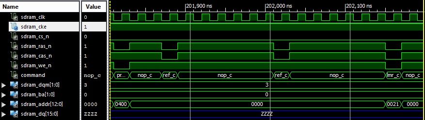
Writing an SDRAM controller from scratch isn’t for the fainthearted – first of all you really have to know how SDRAM works (RAS, CAS, precharges, refresh cycles), and because of the high speed and accurate timing required you also have to learn some of the finer points of FPGA off-chip interfacing. In addition, most publicly available open cores are very complex – for example just the RTL core of the sdr_ctrl controller on opencores.org adds up to over 2,700 lines of Verilog. Even if it is not an accurate comparison metric, [Michael]’s controller is only 500 lines long.


Here’s mine: http://ladybug.xs4all.nl/arlet/fpga/source/sdram.v
Implements read/write bursts, keeps multiple rows open as long as possible, and can delay refresh if RAM is busy transferring data.
Nice one! Will take a look.
I used your controller, it’s very nice but it has some bugs:
– you sample incoming data on wrong clock edge
– accessing address in sequenc 0x10000, 0x20000, 0x30000 one after another will cause invalid address on the last one (RAS not updated).
– wrong_row signal is one clock too late
– if you want to pack registers into IOB, you need to improve some places
I don’t get it. Why bother with some expensive chips and weird programming languages when it can be done in Arduino using simple bit operations.
not sure if serious or trolling…
Good luck implementing an SDRAM controller on an Arduino.
Well this wasn’t quite an arduino, but I did write a bit-bang SDRAM controller for a fast/modern 8051 microcontroller – I also managed to squeeze in VGA, 80186 CPU and most of the chipset emulation in there too while I was at it… :-)
http://www.fleasystems.com/flea86.html
Regards Valentin
Th3DarkCoder:
Tell me how fast your Arduino needs to be to read or write SDRAM at 200 MB/sec. What if, at the same time, for each SDRAM read or write, you also had to do 50 independent SRAM reads or writes, 50 16×16 multiplies, and compute 200 arithmetic and logical expressions?
Speed
My wife wanted to buy a doorstop for the bedroom, but I told her why bother with a specialized doorstop when we can simply use an Arduino ?
I would have a hard time believing that the Audrino digital I/O
calls can meet the timing of a SDRAM self-refresh cycle.
Refresh 64ms for 8192 = 7.8us between refresh. Audrino digitalWrite()
4us and you’ll need multiple of them to toggle clock send command etc.
Ha ha ha haaaa! Nice.
An Arduino?? That’s overengineering it by a mile. A few transistors + a roll of duct tape = SDRAM controller.
I don’t get it! Why bother with some expensive chips and weird programming languages when it can be done by someone else !
This controller only does single 32-bit word reads/writes and opens/closes a row every time, so it’s very slow (compared to SRAM or a more complex SDRAM controller with at least minimal buffering/caching).
I recently wrote an even simpler SDRAM core for the OpenVizsla project. It’s written in migen and special-purpose (it uses SDRAM as a big FIFO, not random access), but it’s much faster (you can get essentially the maximum theoretical bandwidth out of the SDRAM at a given clockspeed) since it uses full-page reads and writes. It also runs on the S6 LX9.
https://github.com/openvizsla/ov_ftdi/blob/migen/software/fpga/ov3/sdram.py
This is the first I’ve seen OpenVizsla, very interesting!
I will certainly take a look!
When did the Spartan 6 become part of low-end FPGA circuits? All I have is a 3E, and even with them, the dev boards are pretty expensive.
This is using a papilio pro, which is a bit less than $90, including a spartan LX9 and a 64 Mbit SDRAM and a usb interface chip. As far as fpga development boards go, $90 is low end.
$11 for a Spartan 6 in TQFP144 sounds fairly low-end.
That’s hardly a complete setup.
“”Maybe I’ll try an FPGA…
… but now I have to add an FPGA and a Flash to hold its configuration bitstream. And I have to figure out how to do in-circuit loading of the Flash. And don’t forget the multiple voltage supplies the FPGA needs.”” — Copied shamelessly from: http://www.xess.com/shop/product/xula-200/ (The sell page of a $55 XC3S200A + 8MB DRAM board in “stamp like” format. AKA the cheapest FPGA dev kit I can find with at least 8MB DRAM on it.)
That said, Lattice’s MachXO2 chips only really need maybe 2 linear regs and some decoupling caps, since they have their configuration eeprom built in. The dev kit for the biggest version is $30, and is very intelligently laid out with lots of conveniently nearby gnd pins so you can wire proper twisted pair lines to get rid of ground bounce, easily changed bank independant VIO pins so you can talk to multiple voltage logic, etc. Oh, and the obligatory FT232 in jtag mode for config. Not Xilinx levels of software polish, but compilations are nearly as quick as Altera, and is available to run under linux.
I have Xilinx, Altera and Lattice devkits & SDK’s.
They each have their merits, and it’s not a bad idea to get familiar with a variety of tools, it gives you options. Likewise, learn both VHDL and Verilog, and maybe system verilog, and be thankful there are so few to learn!
And then of course use something else to generate the HDL ;)
Maybe this is a good place to get some advice.
I want to get into FPGA / VHDL but I don’t know where to start.
I have done most of the curly bracket languages, ironically I haven’t done Java, C, or anything Microsoft.
I am comfortable writing assembly for any micro-controller. I have made small computers in the old times. I can make video interfaces from 74xx logic and I can work with logic expressions.
I want to start with a Z80 and Video interface in VHDL with external RAM / ROM.
I bought a GameDuino which is Spartan 3E 200k but it was a poor choice as it has no real RAM and not enough logic.
I was thinking of the Papilio one 500K with arcade megawing as it has been targeted at this sort of thing but then I saw others around the traps and I don’t what to choose. The Papilao doesn’t have external RAM so it’s not really what I want.
Any advice would be most appreciated.
@rob join the club. Here is what I am thinking of doing. I am going to learn me some VHDL using this book http://www.amazon.com/Circuit-Design-Simulation-Volnei-Pedroni/dp/0262014335/ref=sr_1_1?ie=UTF8&qid=1381554159&sr=8-1&keywords=volnei+a.+pedroni.
Then I plan on working through this book
http://www.amazon.com/FPGA-Prototyping-VHDL-Examples-Spartan-3/dp/0470185317/ref=sr_1_2?ie=UTF8&qid=1381554227&sr=8-2&keywords=pong+p+chu
The Hamsterwiki is one heck of a resource when you run out of inspiration for new things to try out. Again my language of preference is VHDL still the Defacto language in regulated industries such as medical. Verilog apparently is used by every sweatshop semiconductor company in the sillycone valley.
I hope these pointers help.
For the cheapest available fpga board (without dram) go look up the “MachXO2 breakout board”. They’re only about $30 USD direct from LatticeSemi. Otherwise get a papilio one if you want dram + fpga. (MachXO2 is a very nice chip, it’s killer feature is that it has its configuration eeprom built in – just needs some local decoupling caps and power to use – so ideal for small simple applications.).
Otherwise for more serious Xilinx fpga dev (on a budget) check out the ztex.de boards. These have 64/128 MB DRAM, plus you get to use the “firm” Xilinx Spartan6 SDRAM controller, since they have the BGA Spartan6 LX on ’em.
These ztex.de “usb-fpga” boards are more or less built around the cypress FX2, which is an interesting chip in its own right. (8051 + /w all bells and whistles + dedicated fifo), with an independant fast bus capable of streaming from fpga to USB 2.0 hispeed at realistically >30 MB/s without going through the ‘8051 (1.11 version boards) or easily >40 MB/s (1.15 boards with auto-fpga configuration, allows use of fx2pipe on linux which can completely stretch USB 2.0’s legs, the 1.11 boards need the 8051 to configure the fpga, and the ztex fx2 firmware (whilst totally awesome in its own right!) is based on libusb which just isn’t as fast as fx2pipe, which talks directly to the linux kernel usb driver.).
The 1.15 series ztex boards connect the full 8051 internal bus to the Spartan6 via dedicated pins, whereas the previous boards mostly just connect the dedicated fast fifo bus.
This article suddenly makes the non-sdram controller compatible non-BGA spartan6’s extremely interesting – most notably the Papilio Pro.
The $200 gizmoboard has a FT232H fifo chip on it’s “prototype board” which in theory is capable of full USB 2.0 hispeed, (in synch parallel mode, not in the JTAG mode that everyone always has it connected for fpga-feeding duties) although I had trouble getting reliable data along a prototyped 8 bit synch bus, since you have to run it at 60 MHz, and that’s really pushing it for a parallel bus via hookup wire… The fx2 can run in 16-bit or 8-bit mode, and 16 bit @ 30MHz is *much* easier to get working than 8 bit at 60 MHz.
The fx2 can also be had for about $10 in 56pin version from ebay, just be aware that the 56-pin version really only work in “slave fifo” mode, and you really to connect them to an fpga to use them. (don’t get distracted by the “GPIF master mode” in the datasheets! It’s cool, but for some reason, the input control pins aren’t connected on the 56-pin fx2 varients! It still works if you use it in fixed packet bursts though…)
Anywho, gizmoboard + papilio pro would be only about $300 USD, add a hard drive (gizmoboard is an amd64, will run ubuntu desktop and talk to a SATA hdd) and streaming possibly 40 MB/s of your choice of ADC chips to a big hard drive reliably starts looking easily doable, on an unbelievably small budget… Damn, I’m going to have to give it a try now…
IF that FT232H can be interfaced properly to… But ~ 8 MiB DRAM as a deep fifo on the PapilioPro is about right as the minimum FIFO I’d want between a bank of ADC’s and a linux PC that might go AWOL for a ms or so during a streaming transfer overnight… Those hispeed USB fifo chips are good, but the weak link really becomes the timeout an OS will give you. Linux is measurably about 1000x more reliable than win7 in this regards, even if both are running libusb under java.
With a ztex 1.11a board plugged into a xeon PC running ubuntu-desktop and just using the ztex SDK code (java using libusb), I have been able to stream data at 30 MB/s long enough to completely fill a 12 TB external RAID array — without a single missing packet. *MUCH HARDER THAN IT LOOKS!*.
The point is, that deep fifo’s using DRAM connected to fpga’s are basically not-negotiable, if you’re doing any kind of performance interfacing. This project is awesome, because it implements functionality that makes big things possible.
Just imagine having an oscilloscope capable of capturing a whole day in full resolution, with as many channels as you like: If you blow up your experimental power electronics project, you’ll be able to figure out why – whereas you only get the last burst capture with any off-shelf ‘scope. Too bad if you miss that critical moment when the prototype dies…. But if you have the capture, you might figure out that a bit of errant resonance over-voltaged your power transistor due to a standing wave at just the wrong time…. with that capture, you can design a snubber so the next prototype lives. Without that capture… you simply don’t know what failure looks like, so you can’t make your scope trigger just when it happens….
I wonder if it’ll handle the old DDR-1000 DIMMs…. I’d love to take the old laptop RAM I have and turn it into a very physical RAM disk. I think I have a couple of gigs that I can turn into swap space for a Raspberry Pi.