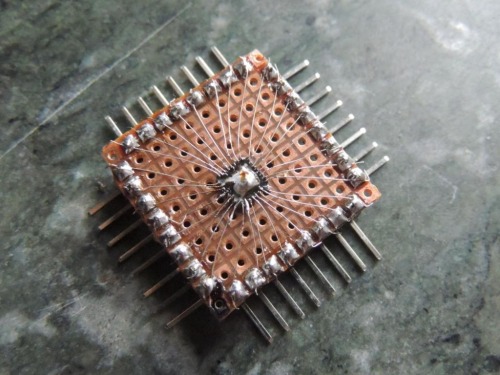
 What do you do when you have ATMega328s in QFN package burning a hole in your bug box, but you aren’t set up for SMD and have limited access to parts? You man up and do what [Djpanjan] did: make your own breakout board with solder, right angle header, and many tiny, beautiful wires.
[Djpanjan] says the process is a simple one that requires great concentration. Once he had it broken out, he covered the wires with hot glue to make sure they all stay in place. He programmed it using an Arduino as an ISP and he was able to run the blink sketch without issue. He blinked all the output pins to make sure there were no shorts.
[Djpanjan] says that if he can’t get a breakout for his LQFP-144, he’s going to make his own again. Good luck, [Djpanjan]. We’re all counting on you.
If you’re set up for SMD and etching, there’s always the surface mount breakout route. If not, you can always use magnet wire and protoboard.


Awesome work! Makes my eyes hurt by looking at all the super tiny connections though!
Considering the pitch on those pads I’m guessing nothing about making that was easy on the eyes…
Should think about dropping off the power and ground pins closer to the chip for decoupling. Asking for SI trouble if your chip has I/O line with fast slew rates.
Or slap a 0402 capacitors between the E-pad GNDs and the VCC pins.
I had to do this at work when the wrong part was ordered, something like a QFN16 was cadded onto the board, but the ordered part was a small pitch 16 pin asymmetrical 6 x 2 package.
I’ve had to do the same – for the wires, I uses the strands from some ribbon cable – the individual strands in a standard 0.050 pitch ribon cable are #36, as opposes to #30 wire wrap wire. Also, it pays to solder the wires from terminal to terminal across the chip in one direction first, the cut the wires to length, and solder each pair to the chip, then do the same in the other direction across the chip.
Better yet would be do as you suggest, but solder the wires to the chip pins, and THEN cut out the middle. I believe I have seen this technique before.
Sourcing #36 like this is a great tip. Thanks!
Grrr… I REALLY need to get a decent microscope. This is very simple when I do this at work under the scope. But those scopes are terribly expensive for home use.
I keep meaning to buy one of those low-cost USB microscopes to see if it would be useful in a case like this. Anyone here tried it?
They work fine for looking at solder joints, etc… but they require the scope to be against the subject, so you cannot work under them. Also, the magnification is too high. That adjustment on the side is for focus, not zoom. For soldering work, you only want 10-20x magnification.
I have tried several different things. The best results so far was a digital camera that allowed the macro focus to be on at the same time as telephoto. I connected the AV out to a small LCD monitor. This allowed me to get some working distance under the camera. But it is a bit awkward to look up while soldering and it isn’t stereo, so the lack of depth also takes some work to get used to.
Sadly, with the cost of all the cheaper options I’ve tried, I probably could have just bought a second hand scope. :/
Yea, I bought my stereoscope off of eBay for about $75. It was in poor cosmetic condition, and it didn’t have a platform. The standing base was there with the cutouts for it’s original platform, but no actual platform, so I bolted on a cheap plastic cutting board from the dollar store. Works great!
I played with those USB scopes in a store. They are using some crappy encoder to reduce data rate. There is an insane amount latency if there are any motions around. It is like play FPS close combat on single digit frames rates…
They are fine for inspecting solder joints, but not if you are trying to wire things. If you can reuse their optics with a video camera or higher quality webcam, it might work.
HAD has posted low-cost ways of doing a cheap USB microscope – for instance:
http://hackaday.com/2011/12/08/hack-a-webcam-and-a-film-camera-into-a-usb-microscope/
There’s also this method (probably simpler):
http://www.joetech.com/tag/microscope/
To keep things cheap, buy the webcam at a thrift shop if you don’t have one already handy (also, I’ve found old toy web microscopes – like that old Intel Play – at thrift stores; perhaps rig a better web camera up to one?)…
Again…. finding a microscope is not a problem. Finding one with enough working distance to solder under it is another.
All of these solutions require the sample to be within an inch of the scope.
Wow, looks like a spider web.
Liez! My eyes are burning!
What I would like to see is the pile of duds that didn’t work :P
I know you are kidding, but, given what I know of his work to date, I doubt there is a “pile of duds”. :)
Oh, QFN rewiring… Last year on a board at work I drew a symbol in Altium with “Flip Board” enabled by accident, which inverts the X-axis of your workspace. This resulted in the pins aligning only when the part was on its back. Having spent $5000 on a quick-turn full-spec PCB order, and being quite tight on schedule, we ended up doing this very thing to at least get us through our initial prototype troubleshooting. Effective, but not signal integrity friendly – we had plenty of trouble with stability of the part, with a half-inch wire as its only ground connection.
And that’s when my company instituted comprehensive peer review procedures on all new component footprints…
I have done dead bug mods for 3Gbps CML (Diff) signal – basically a signal booster to fix Si eye open issues. It was important to not make the proto board worse than it is already.
Basically the 0603 decoupling cap was soldered onto the exposed ground pad on the package and to the power pin *directly* – no wires! The ground was connected with thick copper foil to ground pour on the PCB to minimize inductance. The input & output diff pairs were carefully length matched and were very short (less than 0.5 cm) to the main PCB.
Don’t remember if there were series caps for that arrangement. If there were, I would tombstone the 0603 cap on one side of their leads and solder the diff pair wires to top of caps.
The mod was successful. It can be done correctly, just need to understand SI.
I can’t call it a poor man’s microscope since smartphones are so expensive, but using the Macro camera setting on the phone and good lighting with the phone perched above the work surface by having a stack of something adjacent to the work with the camera side of the phone hanging off of the edge over the work area works well for me. Not sure what magnification I am getting, may not be enough for something this small, sorry for the run on sentence.
You Sir, saved my weekend…
I need a breakout board to a DBM01 Bluetooth LE module and was reviving my good ol’ acid kit.
Way easier!
site not responding
…you go to deal Extreme and buy a nano clone for under $10 and get a usb port and 16Mhz xtal as part of the deal.
No need to kill your eyes with the LQFP-144 – get some breakout boards here:
http://www.ebay.com/itm/2pcs-NEW-QFP-EQFP-TQFP-LQFP144-128-SMT-DIP-Adapter-PCB-Board-Converter-F18-/181301047781
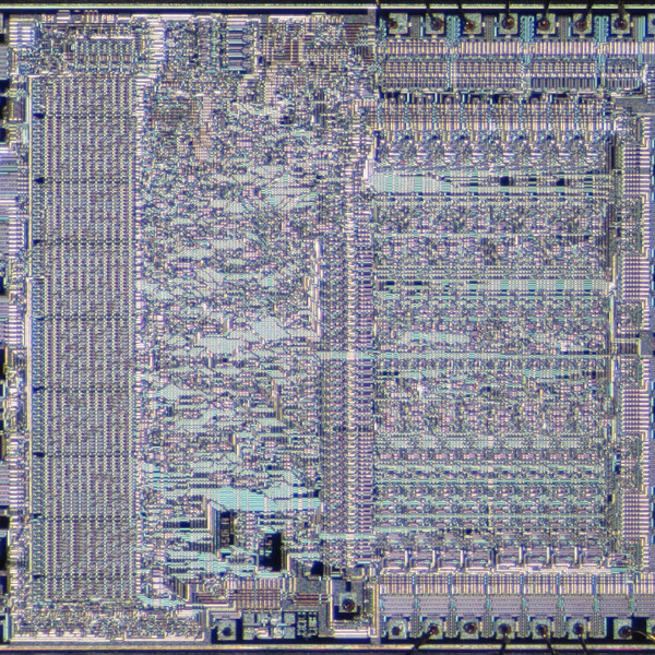
That looks so awesome, and remarkably it closely resembles what many through-hole and SOICs look like when X-Rayed!
I’ve did this for an ARM prototype board some time ago, but I’ve did it for fun also.
http://www.instructables.com/id/ASIIC-ART/
Don’t miss the short story at the ending pictures :)
[]s
Daniel
If I ever get to do that with an LQFP-144 package, I’d rather put it in a frame, and hang it on my wall.
I did it once for LQFP64 with AWG#32 insulating wires to dual row headers as a breakout board. After wiring it up, I gave up on the project.
A couple of years later (also after learning toner transfer for a bit), I transplant the chip onto my (last single sided) PCB. (10 mils tracks/10 mils spacing.) 3 decoupling caps at the corner of the chip with thick tracks to planes inside the footprint
http://www.uplinkchan.net/em/web/Misc%20Electronics/USB/TUSB3210.jpg
I’m unsure if tinning the wires and pins, then using a heatgun to solder the two together would lessen the precision (of using very thin solder and solder tip) in order to accomplish this task.
(Whoops) I meant “to lessen the precision it takes”. I think that that method would’ve been easier.
Not sure if that comment was for my PCB or dead bug.
That’s essentially what I do except the chips already come pre-tinned to ease soldering. Everything done by hand with a temperature controlled soldering iron with a regular tip. No microscopes, reflow oven, heat gun used for this job either.
I pre-tinned the board with hot solder. If there is too much solder, heat and wipe it with a tissue paper – Ghetto HASL. :P
To solder in the 0.5mm pitch LQFP, I add liquid flux (for SMT work) and press donw the pin with the soldering iron essentially reflow/reheat the solder onto the pins/board. This is my way of controlling amount of solder without using solder paste. I tin the soldering iron from time to time and clean it just to make sure it has good thermal contact with the solder joints.
I use a hot air gun at work to reflow a couple of DirectFET onto my pre-tinned PCB, so this works with hot air.
For dead bug breakout, I stick the wire inside the hole on the header side and solder that side first. This anchors the wire and I don’t have to worry about it moving. There is a surprising amount of heat that can travel along thin wire like 30AWG. If you solder the chip side first, it might get undone from the soldering onto the header.
I’m pretty sure I can source 144 breakouts for a reasonable price, as well as asymmetric. Give me a few days to fetch one or two.
heck man cheap these days. 3 to 4 bucks.
http://www.ebay.com/itm/QFP-IC-Chip-TE-QFP44-144Pin-0-65-0-5mm-Pitch-Adapter-PCB-to-DIP-2-54mm-/350564192271
Was gonna plug myself (and still am ;) but I cant beat the ebay
http://shop.diy-scib.org/index.php?main_page=index&cPath=8&zenid=6024e9f6fe277a38750bdbd77b724301
dont have a 144 up yet, but would be about the same price as the 100
What do *I* do? I make or buy the appropriate breakout PCB for the package. But that’s just me ;)
https://web.archive.org/web/20140625064011/http://letsmakerobots.com/node/40451 is a working link, looks like the site sent down in 2016