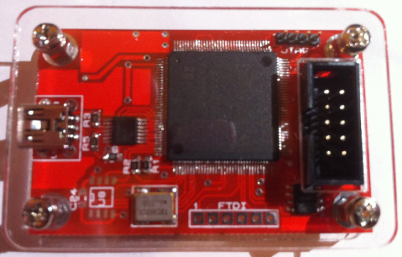
A necessary tool for embedded development is a device that can talk common protocols such as UART, SPI, and I2C. The XC6BP is an open source device that can work with a variety of protocols.
As the name suggests, the XC6BP is a clone of the Bus Pirate, but based on a Xilinx Spartan-6 FPGA. The AltOR32 soft CPU is loaded on the FPGA. This is a fully functional processor based on the OpenRISC architecture. While the FPGA is more expensive than a microcontroller, it can be fully reprogrammed. It’s also possible to build hardware on the FPGA to perform a variety of tasks.
A simple USB stack runs on the soft CPU, creating a virtual COM port. Combined with the USB transceiver, this provides communication with a host PC. The device is even compatible with the Bus Pirate case and probe connector. While it won’t replace the Bus Pirate as a low-cost tool, it is neat to see someone using an open source core to build a useful, open hardware device.


I do like the Zeroplus Logic Analizer, I think it is the best I cant get for that price, About 120 bucks.
This project highlights the need for a low pincount version of the LX family. For many applications, 144 pins is massive overkill.
These FPGA typically have *a lot* of power/ground and configuration pins and can burn up the pin counts in the packages. TQFP144 has 102 I/O, so that’s 42 pins of overhead. Now they could reduce some of the power/ground pins counts. They pay a lot of attention to signal integrity for things, so they put in a lot of power/ground for large # of I/O SSO. (A leaded packages already has a lot of lead frame inductance vs BGA.)
It basically means that the small packages practical (assuming die size not a limit) would be something like a TQFP100. That’s still not a low pin package that you are thinking of.
+ must think that’s often those chip are used in “industrial” production so customer usually go for BGA and 144 pin counts for BGA is nothing.
Some fraction of those supply pins are to support the high number of I/O pins, which can have high dI/dt due to loads and a fast slew rate.
it’s not simply loads and slew rate. But also more significant, the transients (dI/dt) occurring when a wide bus on the FPGA is switching I/O pins simultaneously, either all on, all off, half on & half off, etc. This can happen even when the load is a simple latch. This results in a symptom called ground bounce, when insufficient power and ground pins — even pcb traces — are not available to satisfy the current demands. Each power pin can only handle a limited amount of current before the effects of reactance becomes significant from the pin inductance – which is why you need more as the pin count gets higher. This all falls into the realm of AC analysis of digital design, it’s not simply Hi or Lo logic states. The limited physical ground return path from the insufficient power pins and/or pcb traced induces greater reactance and impedes the current return path. This creates a virtual ground level above the actual ground – as a result, the logic level thresholds become compromised. This can induce logic failures directly into your circuit, even while there is nothing wrong with your components. Ever know why you always need plenty of copper for your ground return connections on any connectors. Ground bounce is one of your worst enemies in the signal integrity world. There’s much to this that I can write in here, I suggest people read more about this — there’s plenty of material online to learn about this.
In a BGA, I assume the chip contacts are on the same side as the Ball Grid Array. In a TQFP, all connections go out to the side.
Personally, I’d like to see a slew of capacitors, embedded in the epoxy. Maybe even a few through-holes in the die, to allow power/ground contacts to reach a common area on top of the chip.
If you make a MK2 pcb.. please bring the spare pins out to some pin headers :) Waste not want not.. Could make a very cool fpga-dev board given the USB port.
Maybe some IO buffer to protect the FPGA could be a good idea.
Yeah, even some of those bus switch chips for bi-directional level translation would help a lot.
I’d say the bare minimum would be some resistor dividers and a zener overvoltage protection circuit. That’d be like $0.25 for some protection which could easily save the FPGA.
Resistor dividers are *slow* for things that runs at tens of MHz, so that they are limiting what the board/part can do (easily a couple of hundred MHz). Zeners add a lot of parasitic capacitance, so they are no good for high speed.
Bus switch devices works like low values series resistors, but their effective values increases non-linearly once they are above their target voltage range. They have additional ESD/overvoltage/undershoot protection and are designed for high speed level translation.
I don’t know if this is a necessary tool for embedded development. If you check one byte on the scope, you can do the rest in firmware on the microcontroller you’re using anyway.
There’s more value in reverse engineering somebody else’s hardware, when you don’t have access to the firmware side of the peripheral.
One of the primary uses of a bus pirate is bootstrapping and debugging microcontrollers, almost by definition you need an extra tool for this.
Now that you’ve bought into needing an external tool, for free you can also get a scope and a logic analyzer.
If your microcontroller is executing software timed loops then there is no way to go in there and add debugging code without affecting the timing
Depends on the microcontroller. Several microcontrollers can be bootstrapped using a simple UART. I also have managed fine debugging through the UART and a few I/O pins attached to a scope.
I think some serious effort should be put into a GUI for these before the rapid hardware updates (my own personal opinion.) The original hardware is very capable, but sometimes I just want to do something simple and navigating all the text menus is a nuisance.
Yes, yes… It’s open hardware, go program it myself! I am not much of a programmer ;) You really wouldn’t want to use my code, much less look at it.
This, the underlying AltOR32 and its underlying OR1k are some of those cooler uses FPGAs we all dreamt of doing. Aw
*awesome work.
A gadget must have a minimum of security when you connect with other circuits, like as PicKitx and iCDX the microchip offer, not to burn yourself or the circuit in which they are connected.
On the question of development of Bus Pirate, I think it should be done a merge with the “Ninja Part”. In fact, there are several other gadgets with similar features that could be merged into the Bus Pirate.