Right now, [The Big One] is using an ATX power supply as a bench power supply for all his electronics projects. It works, but it’s not ideal. The next step up from a power supply from an old computer is, in order, one of those Chinese deals on Amazon, a used HP supply, or for the very cool people among us, building your own. [The Big One] is very, very cool and he’s building the modular bench supply to rule them all.
This is not your $100 china special power supply that [The Big One] would have to buy again in a few months. Inside this massive power supply is a massive transformer and rectifier that fans out to multiple power supply modules. The modules themselves will be based on an OPA548 that will be able to supply up to 3A with current limiting.
Each of these channels will be controlled by an ATMega32u4, with all the fancy stuff you’d expect from the ultimate supply; USB for setting voltage, current, and logging data, a nice LCD character display, and it’s surprisingly cheap; just about $100 for the transformer, and about $50 for each module.
It’s shaping up to be a great build, and with all the features, a power supply that would also make a great kit. If you have any input you’d like [The Big One] to hear, let him know on the project page.


Some really cool ideas here; I hadn’t seen the OPA548 before, and it looks pretty neat. Likewise, I like the modular design.
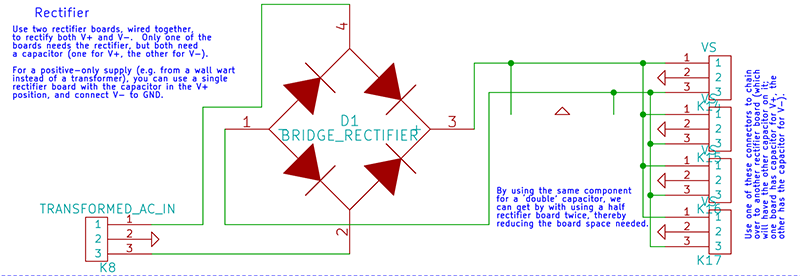
The whole “use two rectifier boards for full wave rectification” thing is pretty weird, though. And if I were designing a supply from scratch, I’d probably have it accept input power from a heavy duty external power brick rather than trying to rectify it myself. Likewise, switching pre-regulation would improve efficiency and reduce the need for lots of heat dissipation capacity.
I am actually looking into using an external supply in place of the transformer right now… there are pros and cons to both.
The ‘use two rectifier boards’ is not quite accurate; it was actually only the capacitors that would be doubled up. There would still be only one rectifier. I have since changed the design a bit to make this more obvious (and have less extraneous board space, too); I just haven’t added the changes to this blog yet.
Cheers
Right, I understand that there’s only one rectifier. But having two PCBs for rectification, one of which just has the cap(s) is thoroughly weird. Why not just make the one board slightly larger?
Incidentally, have you considered putting an analog switch on the positive input to allow for an external control signal to set the voltage? There’s a slew of things you could do with the ability to control the voltage trivially externally with a current or voltage signal.
I am trying to keep the board size down as much as possible for cost reasons. I simply cannot go larger than 10x10cm, and furthermore I am hoping to panelize a couple other smaller designs onto the same board. There is some flexibility there, but a general rule is keep it small.
As for the second bit, I am not sure I understand. I am planning on controlling the + input via a microcontroller / DAC, to allow for arbitrary voltage settings. I don’t understand what an analog switch would buy me in this case.
Cheers
I understand the drive for small PCBs, but when that results in using two PCBs where one would work better, you’ve basically just limited your design’s usefulness to other people with exactly the same constraints – and increased the total bulk of the design in the process. I can’t believe having two PCBs instead of one, with most of one of the PCBs unpopulated, results in a smaller total size (of either PCB area, or enclosure volume).
Having an analog switch would let you control the + input via the microcontroller, or let the user attach a control voltage via an external jack, allowing them to modulate the output voltage however they wanted. Now your benchtop PSU can also be a ridiculously overpowered mono amplifier, or an AM transmitter amplifier, or an arbitrary frequency AC waveform generator, or…
(Reply to arachnidster; I guess HaD comments can only go so deep)
The reason I prefer multiple smaller PCBs is that all of the cheap PCB fab houses give you 10 of them. If I made a regulator board that had everything in the same design, I would have 10 of them and use 1. By splitting things up, I can use multiple pieces, so of the 10 boards I would use 2 or more. This would not be a good idea for mass production, of course, but for hobbyist one-offs it works great.
I see your point on the analog input, thanks for the clarification. I will definitely keep that in mind.
Cheers
Surely the cheap fab houses won’t let you put 2x 10x10cm designs onto the one batch, you would actually end up with a total of 20 boards (10x of one and 10x of the other) so only using 2/20 so you haven’t saved anything, in fact you spent twice as much! Unless you know of a fab house that does what you are saying (links please as I would be interested in that if possible)
I only include one of the two identical boards in my panelized design.
Once I finish up I will post the panelized board… stay tuned!
Cheers
Because 10 cm x 10 cm PCBs are ridiculously cheap, and anything larger is significantly more expensive. 10×10 boards are $15 for a batch of 10 on Elecrow. 10×15? $45.
Multiple 10×10 boards right now are totally the way to go for hacking things together.
A single opamp costs $20. I don’t think the PCB cost for prototype volumes ought to be a significant driver of design.
(Reply to arachnidster)
The op amps cost what they cost. I agree they are on the expensive side, but they also do a lot. I can’t keep costs down in that regard, but I can keep costs down in other places, such as PCBs.
In fact, I would say that the cost of the op amps is a great reason to keep other costs down.
As for the total cost, my design currently costs under $50 per channel for component costs, plus some fixed cost for the input voltage. That’s a lot when comparing to a hacked ATX supply, but try comparing it to multi channel commercial power supplies with voltage + current limiting and positive / negative output on all channels.
One way to save board space is to separate the rectifier and filter on a different board, or even no board.
(Reply to Bogdan)
Yep, my latest design has the filtering caps on a separate (tiny) board. Use two of them and you are good to go.
(I’ll try to post my latest routed board tonight… if I had known this would have been front page I would have done so yesterday… oh well)
I completely, completely agree. Sleazing from a laptop supply can be super-cheap, but even if you go a commercial route, a 300W, 24V supply (which would *almost* meet the 18V, 3A, 6 channel design) is only ~$50, even through Digikey. Which is cheaper than the transformer. I just don’t see the point of mucking around with mains, especially considering the danger.
Do you (or anyone else here) know the best approach for getting a dual rail? As the path of least resistance, I can always go with two wall warts to get a +/- supply… however I would prefer something cleaner (hanging two wall warts off the back is not going to look like a very nice solution).
A switching supply that converts a single DC voltage into +/- is probably not the best; first there is the noise factor, and then of course there is the fact that in all the designs I have seen, the current on the negative side is quite limited.
Any comments / suggestions would be greatly appreciated.
Cheers
You can get multiple output modules – either as inline adapters (laptop style) or as open frame modules you integrate into your case – that have bipolar outputs built in.
Switching supplies that invert don’t have to be any more current limited than non-inverting ones. Concerns about noise are generally overrated, as it’s fairly easy to filter, and a pre-regulation step would allow you to do a much wider range of currents and voltages without overheating.
It depends on how you search for them. If you just naively look for a DC/DC switching supply, and look for a negative output, you’ll be amazed how current limited they are. The maximum you’ll find is like, an amp or so.
But that’s just because they don’t advertise the things you would actually use for negative voltage, high current switching as negative outputs. You just use an isolated supply, or a step-down converter reconfigured as an inverting buck-boost supply. (e.g. http://www.ti.com/lit/an/slva458a/slva458a.pdf ).
But if you don’t know that you can use a device that only lists its output as a positive voltage as an inverting supply, yeah, options can look limited.
Is there an easy way to determine if a supply is isolated or not? For instance I know that some cheap wall warts that I have on hand (el cheapo 12V/1A) are; I have already connected them together as a dual rail supply in testing. However, I would prefer to not have two wall warts hanging off the back of my supply, for obvious reasons.
Something like this http://www.digikey.ca/product-detail/en/LS150-15/285-1812-ND/1918823 looks very interesting, but I don’t know enough to say if it would work for me or not. First, there are two terminals each for + and -, but I really doubt that they are isolated internally, so connecting one of the + to the other – is probably going to be a Very Bad Thing. In the datasheet (http://www.us.tdk-lambda.com/ftp/manuals/ls_manual.pdf page 3), they do show series operation, but it is unclear to me whether they are referring to two separate modules, or two terminals on the same module. Furthermore, in the ‘common ground’ option B, they show two loads. I can assume that this is identical to having a + / GND / – device, but not having any formal training in this sort of thing I am not positive.
Thanks!
“Is there an easy way to determine if a supply is isolated or not?”
Read the manual?
http://www.tdk-lambda.com.sg/pdf/ls25-150_ins.pdf
It’s an AC/DC supply. You plug in AC, and it gives you a DC voltage differential (here 15V) between the V+/V- pins. They’re completely isolated from earth/frame ground – it’s up to you to make that connection however you want. Want 30V? Connect 2 in series and ground the negative terminal of one of them. Want +/-15V? Connect 2 in series and ground the common terminal.
You can’t really ‘split’ the 15V into +/-7.5V easily for high-current stuff unless the current from the + and – supply are matched. Otherwise whatever’s generating that midpoint reference acting as the virtual ground has to dissipate all of that current. (Imagine a device sourcing 1A from 15V – the V+ terminal – and sinking it back to 7.5V: it would only see a 7.5V supply, which is fine, but that 1A of current needs to get back to the ‘V-‘ terminal. It does it through the device providing the 7.5V reference.) It’s a common trick for analog stuff (called a ‘rail splitter’) where the current is low and you don’t care about the inefficiency.
You could imagine doing it with a switching regulator… but of course, this is fundamentally identical to generating the negative supply in the first place.
Thanks, Pat!
Yes, I had read the manual, but it was not clear to me whether or not the V- was internally coupled to Earth / GND. Your explanation really makes sense, though.
I am thinking that this approach will be what I end up doing – grab 2 of those guys, and hook them together in series with GND referenced to common.
Thanks!
Section 4-1, “Isolation Test: Isolation resistance between output and FG (chassis) shall be more than 100 MOhm at 500 VDC.”
Inverting switching supplies are typically low-current because for higher current cases, there’s an obvious solution – any isolated DC/DC module. Ground V+, and poof, you’ve got a negative rail.
Yes, of course there’s switching noise generated when have a DC/DC switcher like that. You’ve still got noise from mains anyway, and a bench supply can burn a bit of power to clean things up. Just generate the voltages with some headroom over what you want, and use a linear regulator with aggressive PSRR in the switching frequency range to clean them up.
I think the design has quite a few flaws… He should not have used a high power opamp, there is not need for a power supply to source and sink current. Second, there is no current regulation…. why would you even consider building a lab power supply without current regulation?
The opamp does support current limiting.
My bad, did not see that feature of the opamp. Interesting. Though it seems kid of imprecise and dependent on the supply value, which is kind of bad.
Also, the next flaw is that the INA169 will have trouble measuring the current when the output voltage is under 3-4V, so basically some range of the positive supply and all the negative supply. The app note shows that way to measure current in both directions, but the common mode cannot be negative.
I am using the INA169 in a bipolar configuration, and so can sense negative current. (See schematic for details). I have tested this on a breadboard and can confirm that it works.
I have not tested current sensing at less than 5v, thanks for pointing out that potential flaw. I will give it a shot at 3.3v (the lowest power source I currently have) and see how well it works.
Cheers
There is a difference between negative current and negative common mode voltage!
(Reply to Bogdan)
I am not an electrical engineer, I apologize if I have mis-used some terms. Would you be able to point me in the direction of something explaining the difference?
To clarify, I have tested the bipolar current sense circuit with current moving in both directions across the shunt resistor. Is that not a valid test?
Thanks for the info.
Let’s put it in a simple way: the INA169 can only work if the Vin+ and Vin- voltages are between 2.7* and 60V, so if your supply outputs -12V it will fry it.
*that is the ideal case, in your design the minimum will be higher due to diode.
Ahh, I see what you mean. Thank you very much for the info.
Do you have any suggestions on an alternate method for current sensing?
Thanks
Alternatively, I suppose I could also reference the INA169 GND to VS-. That would give me 60V of headroom. I would need to change the output circuitry a bit to compensate for the different voltage, but I think that it should be fine.
Does that make sense?
Thanks
See the updated schematic here:
By referencing INA169 against V- instead of GND, we prevent the inputs from ever being negative, and in fact should also prevent them from even dropping below 2.7V (since the output from the OPA548 can never get to within a couple of volts away from the supply).
I could be wrong (and please point any errors out to me), but I think this solves the problems.
Cheers
Hmm, try the link again:
https://cdn.hackaday.io/images/4068181423771743181.png
I did suggest to check my work on this subject here: http://www.electrobob.com/digital-power-supply-part-1-concept/ At the end there are a few other references of digital power supplies. I have a working prototype, but it is at the bottom of a box, it is not of a priority for me.
I am posting this comment for the second time. Seriously, lately more and more of my comments don’t show up and I am sure it does not have any reasons not to. Maybe 1 in 5 never shows up.
Sweet, thank you very much for the link. Looks like many of your design goals and points are the same as mine. I too was initially going to go XMega route, but decided to go back to my tried and true 32u4 along with an external DAC.
I will take some time later to look deeper at your design, and see what I can glean from it.
Cheers
Just as a followup, I have tested the new current measurement technique, referencing the INA169 chips against VS- instead of GND, and it works beautifully. I have tested it with current moving both directions over the shunt resistor, with the input terminals being both +12V and -12V.
Thank you very much for your comments, Bogdan, pointing out the error in the circuit as originally posted. I would have printed boards, soldered everything up, and immediately fried my current sensor chips. Your help is very much appreciated.
Cheers
I am not sure that referring the outputs of the INA to the -V supply is a good idea. Yes, you could always read the current, but then you need to shift that voltage to be ground referenced.
I think the simplest solution here is to make channels isolated(each one has it’s own secondary) and use only a positive supply on each(V- = Ground). That way you can keep your design about the same, even drop out the opamps since you don’t need conversion to the negative range. If you are fine with having each with its own micro and display, then it is great, you can really keep the design.
I am glad I can help.
There are differential amplifiers that can have CMR outside of their supply rails. Use them and a sampling resistor to sense your current. If you set the diff amp output reference point at mid reference voltage of your ADC, then you can read current sink/sourced by the supply for the full range.
Opamps are not the only class of amplifiers with large currents… High wattage audio amplifiers chips are much cheaper. These days there are also class D should you want to have high efficiency for high power applications.
A correctly designed SMPS can be more reliable than a badly designed linear supply. It is a matter of design skills not the topology, unfortunately SMPS does require more.
Yes, the OPA548 includes settable current limits – that is one of the major reasons why I picked this chip in the first place.
Cheers
As for the ‘source and sink current’ comment… my design allows for a single channel to vary from positive to negative. So, given a 3 channel system, you can have one at 12V, another at -12V, and a third at 5v. Or, you can have one at 12, one at 5, and one at 3.3. Or, you can have one at -5, one at -12, and one at 5. Completely configurable via software.
Sure, most digital projects will not need any negative voltage, but once you start looking at audio, it suddenly becomes ‘a thing’.
Cheers
I think this is not great at all. In normal designs you make 3 independent and isolated channels, so that each can be configured which way you want. Sometimes you want isolated channels.
Having a supply that needs to be positive in a circuit but which can also generate a negative voltage is just adding another way in which it can fail. A typical supply will have a diode on the output that prevents the external circuit to inject current which could make the output voltage go negative.
Thanks for the feedback, it is appreciated.
“there is not need for a power supply to source and sink current”
Uhhhhh… what?! Also as the other guys said… there is current regulation check the ILIM pin of that power opamp… he has it take care of. The only downside is the price of those amps… looking at about $20/pce in low quantities
Yeah those guys are pricey… if you don’t need as much current you can use the OPA547, which is good to 750mA and costs a bit less, but shares the same footprint so will work on this board too.
On the bright side, that single chip takes care of almost everything (positive / negative output, current limiting, thermal shutdown if something goes wrong, etc). The total cost per channel is currently under $50 (in fact the last time I looked it was just about $40), which IMHO is a very good deal. By doing everything with discrete components you may be able to get a lower price, but at a substantial increase in complexity. There are tradeoffs to everything in a design…
Cheers
There are trade-offs indeed. For example I would prefer an opamp + power transistor because that is so much easier to scale in current.
In that design, how would you accomplish current limiting? If you have any schematics of such a design I would be very appreciative. I picked the OPA548 because it seems to do everything that I need in a single package. I am just a hobbyist, I am not an electrical engineer, and everything I have done with electronics is self taught. I have a lifetime of learning still ahead of me!
That design is just okay… I’m assuming you’re taking the output of the 2x BJTs/FETs and feeding it back into the input to the opamp’s input comparing it to 1/2Vcc voltage reference… off a voltage divider. All the current is flowing though the transistors and half the voltage drop is over them… that’s guaranteed max efficiency of %50… the transistors heat up
http://upload.wikimedia.org/wikipedia/en/archive/1/1e/20121201033903!Pushpull.PNG
This guy
Thanks for the info / schematic, MachineHum. Always very interested in seeing new (to me) designs.
Cheers
https://www.youtube.com/watch?v=CIGjActDeoM
EEV Blog #221 and start at about 20:00
It gives a good example of a current limiting circuit. If you go back about 5 mins earlier it will explain Constant current/constant current systems using op-amps and transistors(and pots based on input voltage) If you cap up the voltage right you won’t need an external reference either
Cool stuff. I just picked up one of those Radio Shack 12V 19A bench supplies on clearance with the hopes of transforming it into a proper supply.
I’m thinking of doing the same thing this afternoon! Planning on posting your ideas/progress with this? I’d love to follow along… I haven’t given it much though as yet.
How about a ‘power supply’ list over on io? Aggregating those, too, would save people looking for ideas some time.
(Is this the right place or should I take this suggestion to the feedback page?)
why linear, why not switching?
Less noise. And also easier to get better stability with switching loads. I’ve destroyed several switching power supplies with high current PWM loads.
Linear ‘v’ Switching for those who didn’t get to work with linear PSU’s.
Switching –
1) Cheap
2) Easy to buy pre-made modules
3) Efficient
4) Light weight
5) Low heat generation
6) Passive cooling
7) Wide range of output voltages limited by power (not current)
8) Electrically noisy due to high switching speeds
9) Unreleasable
10) Higher failure rate
11) Very susceptible to power spikes
Linear –
1) Expensive transformer
2) Having to do the mains (110-240V) wiring
3) Only efficient near maximum output voltage
4) heavy due to transformer and heat sinking
5) All of the unused output voltage is burned off as heat
6) Large heat-sinks and possibly fans
7) Output is limited by total current and not power
8) Highly stable and clean output regulation
9) Highly reliable – will easily last decades
10) Virtually indestructible
11) Highly immune to power spikes and in some cases even lightning strikes
In a switch mode power supply the heat dissipated is the in-efficiency times the power output. ie if you have a 90% efficient SMPSU supplying 100 watts then the heat generated will be about 10 watts. The efficiency of a SMPSU do not vary much with changes to the output voltage.
In a Linear PSU the heat generated is inversely proportional to output voltage for a given current. ie heat dissipation = (maximum possible output voltage – regulated output voltage) * output current. For this reason the PSU becomes far less efficient at the lower end of the regulated output. This means that the wider the range of output voltages you design for – the more heat-sinks that are required. Linear PSU are letter got a limited range of output regulation.
correction: Linear PSU’s are better for a limited range of output voltage regulation.
Then there are “hybrids” that have properties of both, such as a low voltage switcher (buck converter) running off a mains transformer/rectifier and a switching PSU with a LDO on the output to clean things up.
You can also do a flyback (or a forward) and make multiple secondary windings for isolated supplies. That way you are not limited to the power transformer windings.
I use SMPS for most of my design and add filtering and/or use LDO with good supply rejection for post regulation if I need to worry about noise. Haven’t designed in a 78xx for the last 15+ years. They are crap.
While I know its not in the spirit, I have one of those 89$ 10 amp china special’s from circuit specialist that the day it came in it was plugged in with a 8 amp load and has not been relieved of that in a little over 4500 hours straight (powering units during a long term environmental stress test)
Just sayin
As it was mentioned above, it is too expensive to use LDO OPA548 as voltage regulator. There are a lot of regulated DC/DC converters, which can convert high input voltage to low with 80% – 90% efficiency. The OPA548 can additionally take off 1 – 2 volts to make output slim. the whole effectiveness will be much better. I did this type of power supply:
Transformer -> DC/DC on XL4005 adj -> LDO LM138 adj
Even on maximal load there is practically no heat. And there is no noise in the output.
I don’t think that $20 is that bad, considering what it gives you: full range voltage output across 0V with current limiting.
I agree that the efficiency aspect is not great. Thanks for the info on the XL4005 chip, I will have to look into that one as a possible pre-output step.
Cheers
Expensive is a relative term: i can throw in a OPA548 + uC with ADC and DAC inside and bam: nice power supply with current regulation and guaranteed stability. The analog part is $15 for the OPA548. Or you can spend time and design one from parts like opamp + power transistor which might be $7.5. And you saved $7.5 and spent more time on it.If you are building it just for you, in single/few, it’s much better to go for the OPA548 version. If producing millions…. different story.
Honestly, if you’re building it for yourself, saving time probably isn’t your primary motivation. :)
You are right, but asuming you do decide to make one for various reasons, then your time is also valuable. Maybe time is not the most important thing saved here but knowledge, as it is more difficult to design one from parts than to use a ready made one.
Did you read up on, and understand, the limits of the power dissipation of the OPA-series? You won’t be able to pull 3 amps at lower output voltages even if you have an infinitely large & efficient heatsink. The appnote SBOA022 and the “Safe operating area” of the datasheet is important.
Yes, I understand that the max amperage will only work for higher voltages. For me, that is a perfectly acceptable limitation.
Cheers
Props for using the word “ghetto” in your write-up.
The Big One must have black friends X-D