
Last time I talked about how to create an adder in Verilog with an eye to putting it into a Lattice iCEstick board. The adder is a combinatorial circuit and didn’t use a clock. This time, we’ll finish the demo design and add two clocked elements: a latch that remembers if the adder has ever generated a carry and also some counters to divide the 12 MHz clock down to a half-second pulse to blink some of the onboard LEDs.
Why Clocks?
Clocks are an important part of practical digital design. Suppose you have a two input AND gate. Then imagine both inputs go from zero to one, which should take the output from zero to one, also. On paper, that seems reasonable, but in real life, the two signals might not arrive at the same time. So there’s some small period of time where the output is “wrong.” For a single gate, this probably isn’t a big deal since the delay is probably minuscule. But the errors will add up and in a more complex circuit it would be easy to get glitches while the inputs to combinatorial gates change with different delays.
The most common solution to this is to only “look” at the signals (and store them in a flip flop) on a clock edge (usually, just the rising edge). Now the circuit will work fine if the longest delay from one flip flop’s output to the next flip flop’s input is less than the period of the clock. This makes things much simpler to design.
If you need a refresher on flip flops, they are elements that remember a single bit. A D flip flop will remember its input (named D) at the clock edge and hold that output until the next clock edge. There are other kinds of flip flops, like the T flip flop (which toggles state) or the JK flip flop which can perform several functions. With Verilog, you generally won’t create flip flops directly, but will let the compiler infer them from your code.
Let’s jump right in with some examples. I’ll explain these each in more details as we go. Consider this code:
reg myoutput;
wire myinput;
always @(posedge clk)
   myoutput<=myinput;
This would infer a D type flip flop. The compiler will recognize other types, too. For instance:
reg myoutput;
wire myinput;
always @(posedge clk)
   myoutput<=myinput?~myoutput:myoutput;
This would infer a T flip flop. Usually, though, the inference is not this direct. The input might be a logic expression. The compiler can also infer counters which are lots of flip flops:
reg [3:0] ctr;
always @(posedge clk)
begin
  if (ctr_reset) ctr<=4'b0; else ctr<=ctr+1;
end
Just as using the plus operator allowed the Verilog compiler to do the best thing for an adder, the expression above will let it build an efficient counter without you having to worry about the details. You can build a counter out of individual modules that infer flip flops (or modules that your tool provides for you) but it is better to leave the details to the compiler.
Building a Flip Flop
The demo circuit had three distinct parts: the binary adder circuit from last time is already done. Another part of the example design is to provide an output that latches when a carry is generated. Here’s the part of the code that does that:
reg carrylatch;
// latch carry result
always @(posedge clk)
begin
   if (reset==1'b1) carrylatch<=1'b0;
   else begin
     if (carry) carrylatch<=1'b1;
   end
end
In English, this says that when the clock has a rising edge, check to see if the reset line is high. If it is, clear the carry latch. Otherwise, check to see if the carry is set and if so, set the carry latch. It will remain set until a reset clears it.
The Verilog tool will recognize this is a flip flop with synchronous reset. If you get really concerned about performance, you may want to investigate if your FPGA does better with an asynchronous reset and learn how your tool can be told to do that instead. But for now, this is sufficient. The realization will probably be a D type flip flop with a rising edge-sensitive clock input and a clock enable tied to the carry line. The D input will be tied to a logic 1.
Key Verilog Point #2: Blocking vs Non-Blocking Assignments
Did you notice that some assignments use = and some use <=? This is an important Verilog feature. When you are using assignments, you always use the equal sign. If you are writing a sequential block, you almost never want to use the single equal sign, even though Verilog will allow this. Here’s why:
always @(posedge clk)
begin
a<=1’b1;
b<=a;
end
Because the nonblocking assignment (<=) appears, the value of b will become whatever a was at the moment the clock edge occured. That is, all the assignments in the block happen all at one time. In simulation, that means they happen at the end statement since simulations have to pretend everything happens in parallel. In an FPGA, parallel execution is just how the hardware works.
The problem is, if you do not use a non-blocking assignment. Suppose we had:
always @(posedge clk)
begin
a=1’b1;
b=a;
end
The Verilog compiler is smart enough to know that b should equal 1 in this case and has to generate extra circuitry (a latch) to make sure b isn’t set at the same time as a. This can cause lots of timing issues and unless you are sure you need to do it and understand the ramifications, you should avoid it at all costs.
Key Verilog Point #3: Default Net Types
You may notice that some of the variables in the Verilog code are of type wire and some are of type reg. A wire has to be constantly driven to some value. A reg is more like a regular variable. A reg may, but doesn’t always, infer a flip flop. However, you can set a value in a reg and it sticks.
One problem you wind up with in Verilog is that if you make up a name, the compiler (by default) will assume you mean for it to be a wire unless you tell it otherwise. That sounds handy, but the problem is if you misspell a name, it just becomes a new wire and then you can’t figure out why your code doesn’t do what you want.
The answer is to always include this at the front of a Verilog file:
`default_nettype none
This causes the compiler to throw an error if you use an undeclared net. That will save you a lot of debugging time wondering why things aren’t working.
Counting and Dividing
The remainder of the Verilog takes the 12MHz clock and uses it to drive a 16 bit counter. When the counter overflows, another counter increases. When that counter reaches 91, the secondary counter goes to zero. This takes roughly 1/2 second at 12MHz.
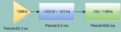 You can figure that out by noting that 12MHz is 83 ns or .000083 us. A 16-bit counter will overflow on the 65536th count (two to the 16 power). Do the math and that comes out to nearly 5.5ms per overflow. If you let the secondary counter go to 91, that will take almost 497ms. If you go to 92, you go over (502 ms). Note that counting to 91 (or 92) only takes a 7 bit counter. A graphical representation of the situation is shown here with the code for it below.
// The 12MHz clock is too fast
// The first counter will / 2^16 (about 5.46ms)
// Then the second counter goes to 91 which is 0.497s
// close enough to 1/2 second for our purpose
always@(posedge clk)
begin
if (reset==1'b1)
begin
  cnt1<=0;
  cnt2<=0;
  half_sec_pulse<=0;
  dec_cntr<=0;
  end
  else if (runstop==1'b0) // don't do anything unless enabled
  begin
    cnt1 <= cnt1 + 1;
    if (cnt1 == 0)
      if (cnt2 == 91)
       begin
         cnt2 <= 0;
         half_sec_pulse <= 1;
      end
   else
     cnt2 <= cnt2 + 1;
  else
     half_sec_pulse <= 0;
  if (half_sec_pulse == 1)
  dec_cntr <= dec_cntr + 1; // count half seconds
  end
end
(Note: as mentioned in the comments below, there’s nothing special about a 16-bit counter. I just wanted to show a nested counter, but since this example doesn’t use the intermediate clock, you could have just as easily made a single longer counter to do the job with one division. The FPGA doesn’t care if you make a 2 bit counter or a 60 bit counter unless you run out of resources.)
This is a form of sequential circuit and the counters will turn into a chain of flip flops when synthesized. Here’s the definition for the counters:
// Manage 12MHz clock
reg [15:0] cnt1;
reg [6:0] cnt2;
reg [1:0] dec_cntr;
reg half_sec_pulse;
The counter declarations look like arrays, but they aren’t (Verilog does support arrays, but these are not arrays). The numbers in square brackets are telling you the number of bits in the value. So cnt1 has 16 bits numbered from 15 (the most significant) to 0 (the least significant).
We’ll use the array-like bit notation and the assign statement to make some LEDs blink too:
// Make the lights blink
assign LED4 = (dec_cntr == 2);
assign LED5 = dec_cntr[0];
Updating the Test Bench
Since the new design requires a clock, the testbench has to provide it. It would be very annoying to have to write each clock transition. Luckily, you don’t have to. Here’s how the clock generation works:
always
begin
#1     clk<=~clk;
end
In English, this says: At all times, you should delay one clock cycle (the #1) and then invert the clock signal and keep doing that forever. Another item to consider is the FPGA reset:
rs=1'b0; // run/stop
reset=1'b1;
#10
reset=1'b0;
This bit of code sets the reset line, holds it for 10 clock cycles, and then clears it.
At the end of the test bench is a 400 cycle delay just to let the counters do something.
Simulation Specifics
There’s one small problem with the simulation. The 12 MHz divider won’t do anything interesting in “only” 400 cycles. It isn’t uncommon to change magic numbers to smaller values when simulating. In this case, I change the primary counter increment to 8000 hex so it will flip every other clock cycle and then changed the test for 91 down to a more reasonable value.
 There are several ways you can do this, but to stay simple, I just commented out the real versions and later I’ll remove the comments and comment out the simulation versions.
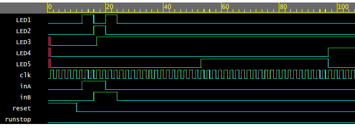
You can see the entire code on EDAPlayground and you can even run the simulation from there. The waveform shown here will appear. If you want to know more about how it all works, check out the video and I’ll walk through it step by step.
Next Time
Next time, I’ll show you how to take the Verilog (which should work since it simulates correctly) and push it down to the FPGA board. If you’ve been paying attention, you should have at least one serious question: How do I tell someone that LED1, for example, maps to the LED on the board? That’s a great question, and I’ll answer it next time. Here’s a clue though: It doesn’t depend on the name of the net. I could have called that signal BigJim and I’d still be able to map it to the LED. If you plan to work along, you can get a head start by installing the open source tool kit now. Of course, if you don’t have an iCEstick, that won’t do you much good unless you just want to dry run the tools.
Selected Tutorials
If you are looking for a detailed Verilog tutorial, try these:
- Doulos (host of EDAPlayground) has a very professionally done set of tutorials
- Another tutorial set up as a self study course
- The creator of EDAPlayground has a series on YouTube that would be helpful, especially if you are using EDAPlayground


nitpick/correction: the period of a 12 MHz clock is 83.33 nS, not 83.33 uS
Well if you stand upside down…. ;) will fix… Oh it is right in the text and wrong in the graphic… That takes longer to fix :(
If you want to go from 12MHz to 2 Hz, why not just make a single counter that counts to 6 million ? Much easier, and gives an exact result.
You can. Especially at 12MHz.
But the length of the carry chain in an FPGA determines the max clock rate (Fmax) of a design. For example, in a Spartan 6 the carry delay is about 0.1ns per pair of bits – so a 64 bit addition will never run quicker than 3.2ns (about 300MHz) due to logic delays alone. So it is customary to use multiple stages of smaller counters (e.g. 10-bit counters that count 0-999) to keep the clock rate up
When you are comparing long counters against absolute values (eg counter – 11999999) there is also the problem of fan-in. That will need to test the state of 14 bits to generate the true/false value that the downstream logic can act on. But using “if counter_millions = 11 and pulse_per_millon = ‘1’” requires only 5 bits, so can be processed faster, giving shallower logic and higher Fmax.
The optimal design varies based on the underlying FPGA architecture, so what is optimal for one chip might be sub-optimal on another, but the general principal is the same.
Good points, but in this case we’re talking about 12 MHz, and a 23 bits counter, so there’s no problem with the carry chain delay.
If you’re concerned about wide comparisons, a simple trick is to count down, and only test most significant bit(s) to detect when you underflow. Or count up, and test for carry out, but initialize at value greater than 0.
And even if you needed cascaded counters for high speed, the example code won’t work well, because the code:
“if (cnt1 == 0) if (cnt2 == 91)” still requires a wide comparator. You’d have to register the ‘cnt1 == 0’ event first.
I am curious what the advantage is to cascading two separate counters, a 16-bit and a 7-bit when a single counter of the appropriate width will do? As someone who does FPGA development (in VHDL, in my case) and also writes software, I understand that using a 16-bit counter is not a limitation of the architecture (FPGA) and is solely a design choice. For anyone who is new to FPGAs, but is familiar with programming and standard data types, the concept of using multiple, familiar-width counters may be confusing and may indicate that this is the only way to implement such a thing. The ability to make arbitrary length parts/pieces is one of the beauties of using FPGAs.
Hopefully I’m not way off base with my comment… that is not my intention at all. I love seeing these guides, especially these since I have only fumbled through Verilog in the past. I also hope I’m not spoiling a planned “teaching moment” for the next installment of the series.
All in all, a great series so far!
[Artenz] and [Jason] you are right, of course, you can do that. I had originally lifted the clock code from the iCEstick demo and my original plan was to show something going on with the faster clock and maybe even talk a little about clock domains. However, it quickly became apparent that I wasn’t going to have space to do that this (at least) this time. However, I wanted to show a multiple cascaded counter just to have something a little meatier than a single flip flop and a half adder, and the double division was as good a way to do it as any.
But you make a good point. You could easily infer that there is some 16-bit limit here like on a CPU and, of course, there isn’t.
If there is sufficient interest, maybe we’ll do a more advanced series at some point and talk about multiple clock domains, metastability, timing closure, etc. What do you think?
Al, before you get to explaining CDC issues, you may want to cover x-prop issues first so people can write and validate their code safely (I normally reference Mike Turpin’s paper)
And Al, if you do do clock domain crossing issues, can you be explicit about the difference between timing errors (where different parts of the design sees different values on the same net at the same time), and metastability errors, where a flip-flop is unable to correctly sample the signal because of set-up and hold violations.
It really bugs me when people go “oh I’ve got a metastability issue with a push-button input…”. The chance of your button-push occurring in the super-tiny window that can drive a flip-flop metastable long enough cause a metastability failure is your design astronomically small – your switch would wear out before an error could be seen.
The more usual problem is that you are failing to do is synchronise the signal before using it in multiple places in the design… so your chance of failure is then approximately the difference in maximum and minimum routing delay to where the signal is used, divided by the clock rate, – very easy to get a 10% failure rate that way,
This is a big issue when people try to implement an async reset, as different parts of the design come out of reset in different clock cycles – async resets are best avoided, IMO.
Continuing the series with advanced topics would be great. If you’re dealing with FPGAs and have any complexity to the design, the topics you mentioned will invariably come up anyway.
Please do :) 3 and a half years later.
Just to make sure I understand Key Point #2, that means that for ‘<=' the order in which the statements are written doesn't matter so:
always @(posedge clk)
begin
a<=1’b1;
b<=a;
end
is the same as
always @(posedge clk)
begin
b<=a;
a<=1’b1;
end
but when using '=' the order in which the statements are written does matter. Is that correct?
Yep. There’s more on blocking vs non-blocking statements here http://www.asic-world.com/tidbits/blocking.html
So for VHDL users, blocking and non-blocking statements is more or less the same as signal and variable assignment…
if you do a:=b in VHDL, a must be a variable and it’s value is updated immediately. On the other hand, a <= b only updates the value when the process is finished. The BIG difference is that variables are only valid within the process statements.
In Verilog you declare a signal as being a simple *WIRE* or a *REG*ister. This declaration isn’t made in VHDL as the synthesis engine makes that determinations and optimises out any non-required registers to simple logic.
Instead in VHDL you have two distinctly different types of code blocks. a *BEHAVIOUR* contains exclusively – simple non-registered logic and a *PROCESS* contains registered logic. You can put simple logic in a *PROCESS* but you can’t put registered logic in a *BEHAVIOUR*
In a *PROCESS* you must declare the signals that time the transition into registers.
In the website mentioned here – http://www.edaplayground.com there is a simple VHDL example –
library IEEE;
use IEEE.std_logic_1164.all;
entity or_gate is
port(
a: in std_logic;
b: in std_logic;
q: out std_logic);
end or_gate;
architecture rtl of or_gate is
begin
process(a, b) is
begin
q <= a or b;
end process;
end rtl;
This is completely wrong. Sure the syntheses engine will reduce it to simple logic (a BEHAVIOUR) and it will work.
What this code is saying is to get a register (D type Flip-Flop) and connect (a OR b) to the data input and clock the register whenever 'a' changes or 'b' changes. The synthesis engine will realise that a register is not required and remove it.
corrections???
the code above does not generate a flip flop, there is no ‘event’ or ‘risingedge’ reserved words, therefore it’s just combinational logic. Regarding the differentiation you make between BEHAVIOUR and PROCESS, I think it’s also wrong.
VHDL allows you to write the same think using different coding styles. One of them is the “behaviour” or fully parallel mode and other is the process or sequential mode. The process was mainly designed for describing registers but nowadays is widely used for defining the any kind of logic (specially useful when big or complex algorithms need to be described since it allows you to think sequentially). I’d recommend you to read the “A structured VHDL design method” by Giri Gaisler.
Wow, VHDL is the exact opposite with “<=" and "="
"a = b" is used to transfer the *current* state of "b" into "a" at a precise time within a "Process".
"a <= b" is used to permanently assign the state of "b" to "a" as a part of a "Behaviour".
On that note, I am not so sure I want to learn Verilog.
Isn’t it :=, with = being the test for equality?
I always have trouble when I see “if a <= b then" in VHDL. My internal parser sees it as an assignment, and I get a "assignment in a conditional expression – are you really sure you want to do that?" brain-fart.
yeah, no edit button
Well you can always do a <= b within a process…specially when you want to make visible a value stored in a variable :P
For the T flip-flop, your code was:
reg myoutput;
wire myinput;
always @(posedge clk)
myoutput<=myinput?~myoutput:myoutput;
Question is : should the last line be:
myoutput<=myinput?~myinput:myinput;
How can you emulate capacitors and resistors in verilog. I have not been able to find any so far
To over simplify things, think of Verilog and VHDL as for digital-only uses. Capacitors and resistors are more for analog uses. Mentally, treat FPGAs as purely in the digital domain.
Getting a little more complex, FPGAs are typically capable of performing DSP (Digital Signal Processing) which may be what you’re asking? Also, FPGA I/Os can usually be treated high, low, pulled-up, pulled-down, and tri-stated. Maybe what you mean by “emulate a resistor” is to pull-up or pull-down a pin?
Ultimately, I think more information is necessary to answer your question.
kloviaclinks com hack tools is working as I got $65,000 from them.