Last time, I showed you a simple PWM block and an open source UART core. This time, I’ll put these parts together to create a PC PWM output peripheral.
Integration
With working code (working, at least, in simulation) you can add the PWM block to the UART driver to get the first version of the PC-based PWM generator. To keep things simple, for now, you just send an 8-bit hex number to set the PWM output duty cycle. For example, if you send an uppercase A (65 decimal or 41 hex), the output will be at 65/256 or about 25%. It is easier, as I mentioned last time, to use a terminal program that can send hex codes like Cutecom.
I’ll try to keep the initial integration simple, get it working, and then add features. First, you need to instantiate the PWM core:
reg [7:0] pwmduty;
wire pwmout;
assign LED0 = pwmout;
ppwmblock pwm(iCE_CLK, reset, pwmduty, 8'b0, pwmout);
Then just connect the received character to the PWM duty cycle register:
if (received) begin
    tx_byte <= rx_byte;
    pwmduty <= rxbyte;
end
Because of the PCF file, the LED0 output is connected — unsurprisingly — to the board’s LED 0. If you want to experiment with the code, try changing to drive a different LED or maybe even multiple LEDs at once. You can also try using the equal-area PWM instead of the proportional, especially if you can watch the output on a scope. If you do want to hook up a scope, you might wish to change the output (or duplicate it) to one of the edge pins or the PMOD socket.
There are two things to be aware of if you do try to add or duplicate outputs. First, the included PCF file has unused pins commented out with a # character. The latest version of the tools has a way to mark a pin assignment as optional, but without it, the build process will fail if you don’t use a pin named in the PCF file. The second thing is that you must add any port you use to the top-level module (see how the LEDs are done). The names aren’t important as long as the name in the top-level module matches the name in the PCF file.
 I made one other change to the UART demo. I modified the Makefile to understand that the output relied on more than just the
 uart_demo.v file. You can find the whole project on GitHub in the v1 folder.
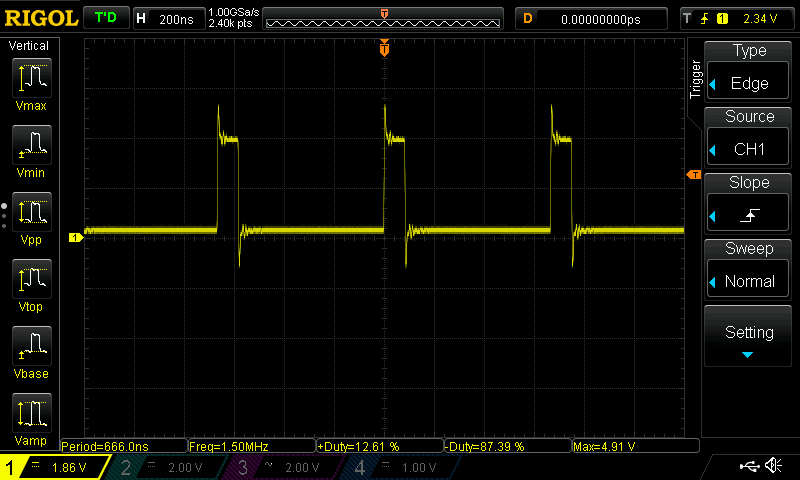
The scope trace on the right shows the output from the FPGA with a duty cycle of 0xA0. You might notice that there is one odd sized pulse in the middle of the series of pulses. That’s because 0xA0 (160 in decimal) doesn’t evenly divide 256. So the counter values (and output states) will look like in the figure.
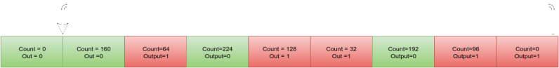
Note that after start-up, the sequence repeats every 8 clock ticks. There is one short high pulse and two double high pulses. Since I asked for 160/256 or a 62.5% duty cycle, the algorithm is generating 5 high pulses for every 8 clock ticks and 5/8 is, indeed, 0.625. The short pulse means you have to get creative triggering the scope if you want a clean display. I’m old school, so I set the trigger holdoff, but you could have used the pulse width trigger to sync on the shorter pulse.
Extending the Design
I want to extend the design to be more useful and to show a few more features of Verilog. In particular, there are three things I want to do to extend the system:
1) Add more PWM blocks with different resolutions
2) Route outputs from the PWM blocks to different places
3) Implement a robust protocol for controlling the PWM blocks
Adding new blocks isn’t difficult at all. The Verilog module pwmblock (and its related wrappers) is like a component. The main file creates an instance of the module using one of the wrappers like this:
ppwmblock pwm(iCE_CLK, reset, pwmduty, 8'b0, pwmout);
It is easy enough to just add more. You’ll need to find space to put the PWM duty cycle, the counters, and the interconnects, of course. You could just make up new registers and wires, but it would be smarter and more extensible to use arrays.
The syntax for declaring arrays is simple:
reg [7:0] pwmduty[3:0];
This defines four elements (0-3) of an 8-bit quantity. The only tricky part is that using an array looks like using bits out of a single register:
dc <= pwmduty[2];
The compiler is smart enough to know that since pwmduty is an array, the brackets indicate an array subscript, not a bit slice. Once you have an array, it is easy to arrange for each component to have its own counters. For example:
ppwmblock pwm3(iCE_CLK, reset, pwmduty[3], 8'b0, pwmout[3]);
It doesn’t make sense to route them all to one LED, of course. The PCF file defines the correspondence between pin numbers on the chip and names in the Verilog file. For example, here’s part of the PCF file:
# Red LEDs
set_io LED0 99
set_io LED1 98
set_io LED2 97
set_io LED3 96
# Green LED
set_io LED4 95
# IrDA port
#set_io RXD 106
#set_io TXD 105
#set_io SD 107
# Pmod connector
#set_io PIO1_02 78 # Pin 1
#set_io PIO1_03 79 # Pin 2
#set_io PIO1_04 80 # Pin 3
#set_io PIO1_05 81 # Pin 4
#set_io PIO1_06 87 # Pin 7
#set_io PIO1_07 88 # Pin 8
#set_io PIO1_08 90 # Pin 9
#set_io PIO1_09 91 # Pin 10
You can use any of the signal names in the PCF file to route the outputs to other LEDs or the edge connector if you want to connect to monitor the output with a scope, for example. Note that only I/O pins in use are uncommented in the PCF file.
New Protocol and Verilog Parameters
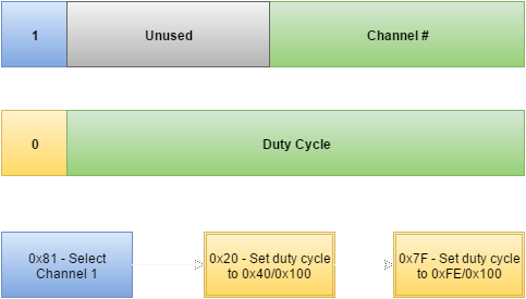
The next problem is how to load up the new duty-cycle registers. Any time you have serial data coming into a device like this, you need to think about what happens if you start listening in the middle of a multi-byte stream. For example, a bad protocol would take the first byte as the channel number (0-3) and the second byte as the duty cycle (0-255). You could have the case where the FPGA resets between the two bytes of a command and then it will be out of synchronization with the PC.
There are several ways to solve this problem. For example, assume that bit 7 of a byte is always set to specify it is a channel. If bit 7 is clear, it is a duty cycle. Of course, that means the duty cycle can only be 0-127.
For driving the LEDs, you can’t easily tell the difference between, say, 50 and 51 duty cycles without a scope. So another possibility is to ensure that all duty-cycle values are even, and multiply the duty cycle the PC sends you by 2 (a left shift will do that easily). You can see an example of this protocol scheme in the figure below.
Alternately, you could set up 7 bit PWM blocks that would be slightly more resource-friendly. Changing the bit length is easy because I used parameters in the PWM block definition. You may have noticed this in the files already. Here’s part of the module definition for pwmblock:
module pwmblock #(parameter CNT_WIDTH=8, DIV_WIDTH=8) (input clk, input reset,
   input [CNT_WIDTH-1:0] increment, ...
This tells the Verilog compiler that, by default, CNT_WIDTH is 8, but particular instances of the module can use other values. In the rest of the module definition (like the creation of the increment argument), the code can refer to CNT_WIDTH instead of a constant number. In the default case, increment uses [7:0] for a total of 8 bits.
If you look at the test bench (on EDAPlayground), you’ll see a test PWM module that doesn’t use the defaults:
epwmblock #(.CNT_WIDTH(10)) dut1(clk, reset, 10'h3ff, 10'h10, 8'h0, ep);
In this case, the counter is 10 bits wide, and increment would use [9:0]. All the places in the code that expect an 8-bit counter will now use a 10-bit counter.
There are other ways you could accomplish the same task. For example, you could use bit 6 of the channel commands as a spare bit to include at the start or end of the subsequent duty cycle byte (that is, 0x80, 0x23 would set the duty cycle to 0x23 but 0xC0, 0x23 would set it to 0xA3). That’s a little harder, though, and not much benefit but it would be worth trying it if you want the practice.
However you tackle the command protocol, you’ll need to change the code that processes received UART characters. Here’s how I did it:
if ( !rx_byte[7] )  pwmduty[pwmchan] <= { rx_byte[6:0], 1'b0 };
else pwmchan <= rx_byte[6:0];
As you can see, the pwmchan register holds the PWM channel number, and it stores the last value from the channel command (after stripping off the extra bits). Then any PWM duty-cycle byte (a byte where bit 7 is 0) goes to the appropriate duty-cycle register using the current channel to select the right element of the array. I also do a shift to multiply by 2 by adding a zero bit:
{ rx_byte[6:0], 1'b0 };
The protocol doesn’t take much to handle in the FPGA. It is robust and efficient (you only need to send a channel command when you want to change channels).
You can find the final project on GitHub in the v2 folder. Although the Makefile handles the build process, if you want to know more about how the open source tools work, you can check out the video from the last time I talked about them, found below.
Results
I routed the first PWM channel out to J3 on the edge of the iCEStick so I could connect a scope probe to look at the real results. Below you’ll see the output at 50% (40 hex) and 12.5% (10 hex). Remember, the percentage gets multiplied by two, so the two scope traces represent 128/256 and 32/256.


The text is tiny, but the scope is showing the positive and negative duty cycle measurements near the bottom of the screen. The output is proportional PWM, so note the frequency changes (about 6 MHz at 50% and 1.5 MHz at 12.5%). These numbers make sense because the base clock on the FPGA is 12 MHz. These percentages work out so that there is no error (that is, the duty cycle count evenly divides 256). In cases where it does not, the fractional parts will cause the square wave to bounce around (you’ll see ghosting on a scope with persistence or just have trouble triggering). That’s normal because the fractional part gets distributed over multiple cycles.
Obviously, the real benefit to this would be to send data over the serial port from a piece of software to control holiday lights, motors, fans, or some other useful PWM function. If you changed the UART code to work on some external pins, you could control the PWM from a microcontroller like an Arduino or a Raspberry Pi.
No CPU?
Can you do PWM with a CPU? Of course, you can. Especially since many CPUs have dedicated logic to produce a certain number of PWM channels. Of course, if you need more PWM than your CPU provides, you’ll have to do it in software. That’s possible, but it isn’t nearly as efficient, especially for lots of channels.
With the FPGA, you can add many PWM channels with no change in performance at all. You could even give each channel its own UART if that made sense for your application (and you can squeeze it all into your selected chip).
Once you have a UART on the FPGA, you have lots of options. Digital input and output would be simple. PWM can be used to drive lights or motors. You could even use it to drive servos. The limit is your imagination, your skill with Verilog, and your access to ready-made cores.


Thanks for the write-up! I did something similar to try and control a led matrix, but I didn’t have the UART part so I didn’t go much further than displaying something static. I’ll have to give it another try sometime.
http://burnt-traces.com/?p=226
Hi
Great article. It would be great to read PWM signals. This would then open up the possibility to make a device that goes in between servos and the receiver. Like a flight computer etc.
I have found some read PWM code below but its in VHDL not my strongest language by a long shot. Would it be difficult to convert this to Verilog?
http://opencores.org/websvn,listing?repname=serial_div_uu&path=%2Fserial_div_uu%2Ftrunk%2F#path_serial_div_uu_trunk_