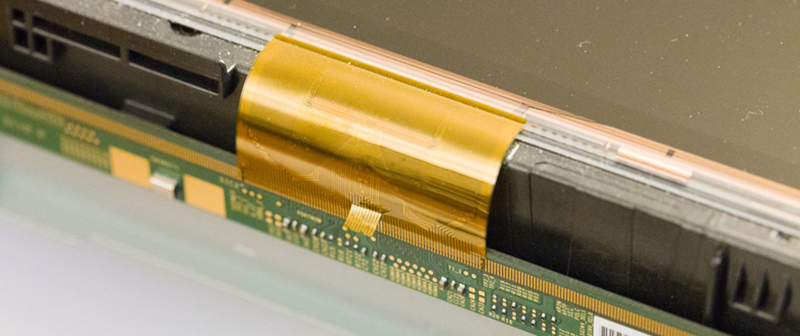
[dyril] over on the EEVblog has a broken LED TV. It’s a fairly standard Samsung TV from 2012 that unfortunately had a little bit of corrosion on the flexible circuit boards thanks to excessive humidity. One day, [dyril] turned on his TV and found about one-third of the screen was glitchy. After [dyril] took the TV apart, an extremely strange fix was found: shining a light on the corroded flexible circuit board fixed the TV.
The fix, obviously, was to solder a USB light to a power rail on the TV and hot glue the light so it shines on the offending circuit. Solving a problem is one thing, though, understanding why you’ve solved the problem is another thing entirely. [dyril] has no idea why this fix works, and it’s doubtful anyone can give him a complete explanation.
The TV is fixed, and although you can’t argue with results, there is a burning question: how on Earth does shining a light on a broken circuit board fix a TV? Speculation on the EEVblog thread seems to have settled on something similar to the photonic reset of the Raspberry Pi 2. In the Raspberry Pi 2, a small chip scale package (CSP) used in the power supply section would fail when exposed to light. This reset the Pi, and turned out to be a very educational introduction to photons and energy levels for thousands of people with a Pi.
The best guess from the EEVblog is that a chip on the offending board handles a differential signal going to the flex circuit. This chip is sensitive to light, and shutting it down with photons allows the other half of the differential signal to take over. It’s a hand-wavy explanation, but then again this is a very, very weird problem.
You can check out [dyril]’s video demonstration of the problem and solution below. Thanks [Rasz] for sending this one in.


Aren’t some diodes made from point contacts with oxidized metals? Could he be getting a photodiode effect in one of the traces (or a solder joint)? I know next to nothing about the chemistry etc of diodes, transistors, etc. so this is just extremely wild speculation.
yes, copper oxides have photoelectric stuff going on, that seems possible to me.
Yes Copper on copper oxide forms a diode, and diodes are light-sensitive.
What probably ends up happening is a diode has junction capacitance, and biasing the diode with some amount of current changes that capacitance, and shining light on it causes that biasing current which changes the capacitance enough that the signal can get through.
The other option is that the light causes a photoelectric effect which frees electrons, which enables a marginally conductive joint to conduct more, such as in an LDR.
https://en.wikipedia.org/wiki/Metal_rectifier
“Metal rectifiers consist of washer-like discs of different metals, either copper (with an oxide layer to provide the rectification) or steel plated with selenium”
I think you’re SERIOUSLY mixing up various applications of junctions, as well as what junction capacitance actually is. Hint: There are two different kinds, which work through different mechanisms, which first require you to remove minority carriers (weird, but the charge-voltage relation holds), before the second forms across the depletion region (which functions more like a conventional capacitor).
Semiconductor physics lessons aside, I don’t think this has anything to do at all with capacitance, forward biasing, or what I can only assume you take to be photocurrent (all of these things occur under different conditions, by the way). What I believe to be the problem, is that you have oxides forming which create a whole bunch of jumbled imperfect junctions oriented in variety of ways, and that’s a recipe for conducting poorly in any direction. (look up non ohmic contact for examples of this occurring by accident with wire-bonds in chips)
Anyway, when light is introduced, it stimulates pair production in the junctions (not photo-current as in photo-voltaic cells!) where each mobile charge migrates to the side where it is not a majority carrier and allows for current flow across junctions which are otherwise reverse biased (this will also reduce the resistance of a forward biased junction). This is the basic principle behind photo-diode detectors.
Aside:
Photo-voltaic cells are different from photo-diodes as they produce electromotive force. Photo-diodes only exhibit a reduction in resistance in their reverse-biased state. This actually means photo-voltaic cells are forward biased as opposed to reverse biased like a photo-diode, despite what their energy level graphs would imply. This is possible because the ‘bias’ of a junction is dependent on what charges are present at the extreme ends of the junction, not the relative energy levels of the N and P sides.
This comment is so useful that i’ve copy-pasted it into my [text edit RTF] reference documents pool (filed under: photo diode junctions). Thank you, M ^_^
There is a lot of useful info here
Not true that diode don’t produce voltage. LEDs are diodes (as their names imply: Light Emitting Diode). Connect a voltmeter to an LED then illuminate the LED and you will see a voltage indication on the voltmeter. This is well known and easyly verified.
This is true, however it is because the LED is a light sensitive diode as opposed to a simple diode. Transducers that work to emit a signal usually work in the reverse direction as well, i.e using a speaker as a low quality microphone.
*because the LED is a light *emitting diode as opposed to a simple *photodiode.
Also, I should have said: An LED is more similar to a solar cell than a photodiode sensor.
Except absolutely all diodes are light sensitive to some degree. The ones that aren’t are only because they’re in an opaque enclosure specifically to prevent light affecting their operation.
ALL these devices are diodes. But there’s more to it.
Photo-voltaic cells are made such that the amount of photo-current produced by pair production (when exposed to light) There’s actually some really neat stuff they do with multiple semiconductor materials and their band-gap energies to make it more likely that an incident photon will produce a pair right at the junction between N and P. I’m fairly certain that you have to be careful with the design of these cells, as they are forward biased by the charges that accumulate, and thus must produce more photo-current than is consumed by forward-flowing charge in the diode. Led’s just happen to be set up in such a way that all this can occur, albeit inefficiently. There’s some really cool stuff that goes on with LEDs, especially stuff with impurities that produce intermediate energy levels in what would normally be the band-gap, though how this works and how it improves the diode’s light emission is something I don’t know a tremendous amount about at the moment.
Photo-diodes however, which are NOT LEDS, are reverse biased diodes which exhibit a reduction in resistance when exposed to light, due to the production of pairs of electrons and holes at the junction, whenever a photon is lucky enough to land there. Because the diode is reverse biased, its energy levels are set up such that these carriers migrate to produce additional current, thanks to the electric field present in the depletion region. This manifests itself as an increase in the reverse bias current (not *exactly* like a reduction in resistance, but it’s pretty similar), and can be done (in theory) with any old diode, like those encapsulated in black plastic, by drilling a hole and letting in light. With diodes designed to measure light however, you want to increase the probability that electrons will land near the junction itself, and one trick is to insert some intrinsic semiconductor, which stretches out the depletion region.
An aside, for those interested:
A photo-diode and photo-conductor are different, despite both measuring light. A photo-conductor is not a diode, and contains only one kind of semiconductor material (like a hall effect sensor, those are fun!), either P or N. Incident photons merely create additional mobile charges, and thus reduce the resistance of the given material.
EDIT: first sentence is incomplete and should read:
Photo-voltaic cells are made such that the amount of photo-current produced by pair production (when exposed to light) is maximized.
Seems pretty unlikely. An inadvertent, PCB + solder-based diode, would have a lot of leakage surely, and at the low voltages and fast signal levels, not sure it’d make a difference.
Of course doesn’t mean I know what HAS caused it, but I don’t think that’s the thing. It’s more likely to be something silicon, which can be very light sensitive, easily enough to affect functioning. In the early days, people used to cut the tin packaging of a transistor open, to make a phototransistor. There were also experiments making camera sensors, by taking the top off of RAM chips.
Would be interesting to mask off bits of the circuit with black paper, or to move where the light shines, try find the exact component it’s affecting.
OTOH if he’s fixed it, in such an unlikely way, in practical terms it’s probably best not to mess. Wait til it’s obsolete. Offer up lead-based incense to the gods of technology and give thanks.
No need to mask, just use a laser pointer…
Faster signals actually can overwhelm a diode, as the junction capacitance means that the diode can’t recover fast enough to pass it.
I’m wondering if the second commenter on the forum post might be right… cdev asking about the possibility of an ambient light sensor… Could be causing the TV to attempt to compensate for bright light in the room and increasing power to the backlight LED’s… and that maybe ones for just that section are right on the cusp of failure, so the increased power going to the screen/backlight are kicking in. further isolation of which component is being illuminated near that cable would be interesting, too.
Backlights on LCD TVs are commonly CCFL tubes that run horizontally across the width of the screen. I would think that one of those in the beginning stages of failure would cause a lighter/darker patch across the screen rather than vertically. I did have a Sony LCD TV which had a glitchy vertical patch similar to this one, the fix was to wedge something between the flexible ribbon and the frame to make a more positive contact.
Modern LCD TVs (including this one, described as an LED TV) use LED backlights. Older ones used CCFL tubes. A common failure in those was the inverter blowing, not quite specced generously enough. I noticed that with an old TV / monitor, if you looked very closely, at the right angle, you could just about see the picture, black pixels on black, after the backlight failed.
This has absolutely nothing to do with the backlight or the ambient light sensor. The LCD is split into sections and if you look closely, the ribbon he is shining the light on goes to thr dodgy section. I am in favor of the photo electric effect here. He is reducing the resistance in one or more traces, allowing the signal to get through. Considering the sensitivity of something like this, even small errors on the incoming signal will degrade the image… so it makes sense that copper and copper oxide in the ribbon are acting as a photo electric device and allowing signal to jump the bandgap.
It doesn’t look at all like back ligthing problem. Really look like some bad contact. The oxidation creating a junction effect and the light increasing this junction conductance is, I think, the best guess.
Weird shit happens sometime with circuits. I hade a circuit that stopped working when I closed the lid on the box, but eventually I figured out that the sunlight on my workbench was needed for a 4017 chip to work (it stopped responding to pulses without direct sunlight). Swapped the chip for another and never had the same problem. Really annoying problem to locate.
Aye, reminds me of that Powerpoint from NASA’s electrical engineers about some of the stupid crazy fails they’ve had over the years – possibly containing the quote “I’ve never come across a datasheet that was completely accurate for anything larger than an 8 pin IC”
I can’t find the slide show for the life of me.
555 timer is 8 pin IC and I get weird shit from it now and then. The datasheet is not accurate for that 8 pin IC.
Your turn NASA.
Well yeah, but that’s probably the worst example ever, considering the number of variants and probably manufacturers combined with its popularity! Why not a 2N2222 transistor while you’re at it? :)
No one mentioned variations. Even from the same factory there can be minor variations in different batches.
Not that the wording would in any way, shape or form imply that all datasheets for 8-pin ICs are accurate.
Your turn, Captain Reading Comprehension.
Absence of evidence / evidence of absence.
It’s kindof annoying, being clever and understanding basic logic, in a world where people generally aren’t and don’t. Don’t you find?
That is about a hackerly a hack as I have ever seen
Please let this become a common phrase
Blogged that.
No kidding! This is the real deal. Love this stuff!
my old thinkpad has the exact same defect…maybe this will help me too!
maybe. but your problem is probably related to metal fatigue in the ribbon cable due to opening and closing the lid. :-)
What happens is that the observer thinks for sure he knows cause/effect and the linkage between them . Often, it isn’t even close
So, we need a Heisenberg Compensaeor?
yeah it’s got something to do with the photosensivity of silver chloride or some other metal oxide, halide, etc. It’s probably acting as a photoresistor or something, acting as a resistor until it’s bombarded with photons
Witchcraft I tell you witchcraft!! But just a question, since the TV has a backlight couldn’t he use some fiber optic cable to leach light from that source instead of the UBS light doohickey he came up with?
It depends if his workaround is needed to light up the backlight in the first place.
A better solution is to redo all solder joint that look oxidized.
I expect my success rate at soldering one of those (kapton?) flex connections would be about 2 or 3 negative orders of magnitude.
I wonder if a laser pointer could be used to pinpoint the exact location of the anomaly….
This is something done in the semiconductor industry to find marginal circuits. A laser slowly rasters the die while the chip is running diagnostics. The diagnostics are set up to twiddle a pin when they detect a fault. When the fault pin asserts, the laser position is recorded. The position will correspond to the transistor in the marginal circuit.
This works because of the photoelectric effect. Hitting a transistor with the laser biases the transistor slightly and changes the switching characteristics of the gate it’s involved in.
Nice info! Thanks!
I think this is also one of the techniques for hacking on the silicon level (with FIB).
I wonder if it’s dependant on a particular frequency of light?
Silicon likes (infra)red most I believe
Silicon is almost transparant to IR above 900nm. So probably more like orange/red.
removing is the ‘easy’ part :), aligning and permanently fixing replacement (dont get me started on sourcing replacements) is the problem. Iv only seen machines that do this in China. as far as Im concerned this is BER.
I used to work at Heathkit (remember them? :-) as a technician. We saw all sorts of hacks. I opened up an H89 computer one time and discovered a pencil jammed in between the circuit board and CRT. It was obviously a bad solder joint, but made me laugh.
I use a clothespin on one of my CP/M disk drives. (broken/missing door latch)
My H89 had an intermittent in the CRT tube. When it wouldn’t light, I’d pick the computer up an inch and drop it. Also, sometimes when I turned it off, a green dot would appear in the center of the screen for several minutes, even if I un plugged it. Turning it on then off again would make it go away. Also, my flyback transformer got leaky causing an arc. I used some fishing line to pull the high tension lead away from the thing it was arcing to. Sometimes i’m sorry I gave it away…
Nearest I can see is that this is caused from the resistance of the membrane cable, once corroded its resistance has gone up, reducing the voltage of the signal below the triggering voltage of the pixels. Bombarding the corrosion with light, at the Cu / Cuo2 junction causes a photo-voltaic response bringing the voltage back above the trigger voltage.
Sort of like the Serviceman’s Paradox?
Where the equipment doesn’t malfunction once the Serviceman arrives?
B^)
Simply make a fiber to conduct the light, or a LED on a piece of wire, then shine on each part until you found the one that does it.
Seems simple.
Then you look up what part it is, and you’d be a long way into solving the mystery.
Well, he’s good at keeping secrets then.
Did YOU look at the video and read the article is my question.
He shines it on a broad area, and the article is about the discussion as to what is actually happening.
To find out the exact part you need to do something else than flood it with a wide beam. and so I suggest that instead of guessing if it’s a part or the cable itself and if it’s a part what part you simply make a narrow beam to exclude areas and find the one specific thing that causes it.
Dammit. I wish I’d known about this when my Sony E-reader gave up.
Had the “half a screen” bug common to PRS-505 units, yet the thing worked sometimes when in bright sunlight with the case off at certain angles. Never thought it could be light sensitivity.
Perhaps the problem is actually the interconnects not the chip, some FPCs use copper/nickel nanoparticles so the effects could be similar here.
As a samsung dealer that failure is insanely common. It’s not just “humidity” it’s a poor design that fails easily. I see that kind of wide vertical stripe failure on at least 30 out of 100 sets from the 2012-2013 era. They fixed it in the 2014 models, and the earlier models did not have that problem.
1.2 volt output? couldnt you connect a nicad or nimh cell directly to the output of the chip and power the board that way?
Wrong thread?
EP (elaborate please). We’er not all versed in the 17.576 TLAs
Could it not be from the heat from the light? Expanding the copper ever so much making contact? I use a LED flashlight all day long and that sucker can put off some heat. The TV starts working when it has a direct hit of light. Just an idea.
breathing would provide more heat than led light
This reminds me of the Story About Magic in the jargon file: http://www.catb.org/jargon/html/magic-story.html
A switch with only one wire connected to it would, when flipped, crash a computer.
i house with decent air conditioning should take care of the moisture that would lead to those problems.
you dont mention where you live so it may be possible if you live in the south where the katrina flooding happened it may be possible that your house was repaired with shoddy drywall
http://www.cpsc.gov/en/Safety-Education/Safety-Education-Centers/Drywall-Information-Center/How-can-I-tell-if-my-home-has-problem-drywall/
if the metals in your house are degrading like in above site it could be possible that the same fumes that reacted with the other stuff caused the degrading of the contacts in the tv.
If you are working with a high gain amplifier, and having difficulty ridding yourself of all AC hum, try turning off the overhead fluorescent lights! If the hum goes away, my experience has been that it is not EM field pickup, but photosensitivity. I do not care if it is modulated conduction or photoelectric generation at work. In the past, it has almost always been glass packaged diodes as the culprit. My sniffer/finder is a coin cell + 555 running 200-300 Hz + white LED + opaque plastic soda straw. Maybe someday I’ll modulate my green laser pointer, no doubt an even better finder.