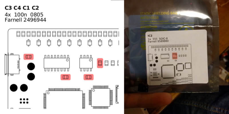
When boards were larger and components mostly through hole, designers could put a lot of information on the silk legend – reference designator, values, additional text and so on. But with surface mount components becoming smaller and board real estate at a premium, modern boards do not have a lot of information marked on the silk layer. If you are building and distributing a short run of kits, perhaps for a round of beta testing, then [Adam Greig]’s StickerBOM python script for KiCad can be really handy. StickerBOM is a KiCad BOM exporter designed for people stuffing boards by hand. It generates a PDF for printable sticky labels, where each label reflects one BOM line from a supplier. You then stick these labels on the bags from your supplier, and they show you where the parts go.
The labels get printed with the reference designator, quantity, component value, package, vendor and part number. It also adds a drawing of the PCB with the relevant parts highlighted for easy location identification. To use it, schematic symbols must have the supplier field and part number added. The script can be run from the command line, or from the BOM manager in eeschema. The script is set up for Avery L7164 labels, but this setting can be changed. It’s still work in progress so there’s a couple of bugs to be aware of. It cannot process the bottom layer of the board, and the result is only as good as the data you provide. And if you have a large board with components spread all over, the resultant graphic printed on the label may not be ideal.
We are hoping this, and other scripts such as the Part generator and Cost spreadsheets or the script for mechanical CAD export, get added to future releases of KiCad. The KiCad version 5 Developer’s road map document already has some really nice feature additions in the works.


Whoa! That’s fantastic!
….. Switches back to using KiCad
Very cool. I’ll try to get it now!
Done that with Protel like 10 or 15 years ago. That’s a good indicator how far behind open source software is when compared to commercial software.
Remember, it’s only free if your time is worth nothing.
Do you have a picture of the protel generated labels? I am curious, since I briefly worked in a protel shop and spent a lot of time searching for footprints on boards I was assembling.
All generalizations suck.
Right!
Protel/Altium showed promise, but was only really appropriate for their FPGA kit simulations.
The software did have an good auto-router that accounted for electrical and thermal limits, but could not really handle simulations that electronics-workbench/mulitisim solved in the early 90’s. For example, anything with an H-bridge would require initial conditions to be set for every line… mulitisim cleaned up many of the Protel99SE problems (mostly copied Cadence’s awesome OrCAD), but for >$5k they priced themselves out of the market.
KiCAD may ultimately dominate the industry, as engineers have not really agreed on an interoperability standard in ages. Like EagleCAD (pre 6.4) it is was not really intended to solve every problem. However, KiCAD can be legally adapted to user demands and customization with regular development languages (hence the wonderful python utilities).
I suspect people will not get features like functional finite element method simulations in KiCAD, but most consumer software still can’t correctly handle SPICE decades after it was implemented.
Not really a good indication at all. It’s a single feature. How many commercial programs have this feature? All? Few? Only Protel? Protel has also existed 7 years longer than Kicad.
You’re rather slow to understand. Open source is ‘free’ not as ‘free beer’ but as FREEDOM.
How many times one will have to repeat it before you understand?
Contributors exchange their time with others time. It is called cooperation and it gives great result.
No, we aren’t “slow to understand”, Brohiem. We understood the phrase the first 100 times we’ve heard it. Shut up Stallman and quit couch surfing! Maybe we haven’t repeated it with 100% accuracy but we understood it.
Let us NOT remind you how an entire city switched to Linux only to switch back to Microsoft.
We don’t want this so called ‘free’, many of us want the DAMN ‘free beer’ before the core team gets ‘bought out’ like Postgrel, Mysql, TOAD.
Serving wheat that has been boiled & semi-fermented then offering us a drink of that FREEDOM isn’t worth the time at my age.
TOAD was never a free software… As Postgresql team was not bought. There were many Pgsql developper out of Sun and it is still in active development. There are a lot of Pgsql developpers at Redhat. Mysql was forked by several companies.
You give the example of a SINGLE case where a city switched back from OS software. I have hundred of example of the contrary. I can have hundred of examples where companies switched from Weblogic / Websphere to Tomcat / Jboss. They never switched back.
> Done that with Protel like 10 or 15 years ago. That’s a good indicator how far behind open source software is when compared to commercial software.
Or that feature wasn’t useful to enough people.
Thanks for the reminder that folks who don’t want to drop thousands on EDA packages to make hobby circuits are idiots though.
That is pretty cool!
I usually just keep an Eagle window open while I assemble. But I would love an option where you could highlight all parts with the same value, similar to the paper method here.
I do the same thing with OrCAD. Open up the layout and search the assembly layer by refdes.
Still it’s a neat idea though, I guess.
From the KiCad developers roadmap
“Study ergonomics of various commercial/proprietary PCB applications (when in doubt about any particular UI solution, check how it has been done in a certain proprietary app that is very popular among OSHW folks and do exactly opposite).”
Sounds like at least one of the KiCad devs is fed up with the Eagle UI…
And is taking cues from Linus Torvalds, who designed git with the primary principle of “Do exactly the opposite of CVS/SVN”.
Something Eagle has (which I personally use A LOT) that KiCad lacks (at least when I tried KiCad last) is a command line. I barely use the UI when routing, as I have bound shortcuts to commands that I use often and can use the command line to access the functions I want. And since I can set a custom command for my shortcut, I can customize my work very heavily. It was years since I last clicked the “route”-button.
That is one of the reasons I don’t use KiCad (not a very big reason, though, as I find KiCad quite nice to route in). The main reason why I don’t use KiCad is the severily retarded way that KiCad handles components and the connection between schematic symbols and footprints.
I use EAGLE a lot. What are these problems with the UI?
That’s a cool idea, I’ll have to give it a try! Now, to get Digi-Key to apply the stickers to my bags before they ship.. hmm..
I’m unaware of any scripting limitation preventing someone from implementing the same idea in Eagle. The fact someone came up with a good idea neither package implemented in a baseline and choose to code it in the tool he routinely uses, isn’t an indictment of either package. If someone more educated than I can definitively say,No, this can’t be implemented in Eagle scripting.. let the flame wars continue.
But as far as CadSoft and and the KiCAD team, neither are making a dent in Mentor, Zuken, or Cadence market shares while there is plenty of pricing incentive to do so. If you are wondering why people pay so much $$ to those three companies when KiCAD is so great, maybe you don’t quite have the handle on the EDA market you think you do.
In eagle, You could do something similar by running the BOM tool and outputting a TXT file.
Then highlight all the parts the same value and copy the line so you get something like:
“R5, R6, R9, R10, R11, R12, R13, R14, R15, R16, R17”
Then, in the layout view type
Show R5 R6 R9 R10 R11 R12 R13 R14 R15 R16 R17
Such an action will highlight all those devices on your PCB.
It’s not quite the same as the post here.. but it could be a start.
A couple of tips for the Eagle SHOW command: first, you can abbreviate commands. So ‘sh’ works if you’re in a hurry. Second, there are wildcards: ‘c*’ selects all parts starting with ‘C’, ‘c[1-8]’ selects C1-C8. Not case-sensitive.
‘sh @ c1’ highlights C1, and also draws a box and pointer around it.
‘sh @ c[4-8]’ draws a box enclosing c4-c8.
I haven’t quite figured out the numeric range syntax. ‘c[1-9]’ does what you’d expect. So does ‘c1[0-9]’. But ‘c[10-19]’ selects only C1. ‘c[0-1][0-9]’ selects only C10-19. Anybody have a hint?
While KiCad is already fairly keyboard-centric, I’d love to see something similar to the powerful, versatile, scriptable Eagle command line.
That’s really handy! I recently did something similar albeit manually; print the pcb design 30 times, cut them to size, use a red marker to mark the locations of the components and stick em on the component bags / reels.
This takes much less time and is less error prone, thanks Adam!
I do this by hand with a colored highlighter marker, it takes almost the same amount of time and works for people who don’t want to bother with a color printer.
I work on a electronics contract manufacturer for 5 years now. We do use a document for the PCB assembling that look like that sticker , it has the PCB image with each component highlighted in one color and each color corresponds to a specific manufacturer part number. In other page of the document it have the colors with their respective part description. The software we use for that is called vPlan Process Preparation, from Mentor Graphics.
Very nice script, this looks like what I’ve been doing by hand using Gimp for my Cadsoft Eagle designs. This gave me the push I needed to improve my process, a few hours later, I now have a perl script that does it automatically. It’s not as nicely integrated as StickerBom though.
https://github.com/semicolo/SMD-Manual-Place-Image-Generator