Turn Your Laser Cutter Into An SLS 3D Printer

Filament style 3D printers are great, but typically are rather size limited. Laser sintering printers offer huge print beds, but also come with quarter million dollar price tags. What are we supposed to do? Well, thanks to OpenSLS, it might just be possible to turn your laser cutter into your very own SLS 3D printer.

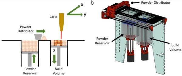
We’ve covered OpenSLS a few times before, but it looks like it’s finally becoming a more polished (and usable) solution. A research article was just recently published on the Open-Source Selective Laser Sintering (OpenSLS0 of Nylon and Biocompatible Polycaprolactone (PDF) that goes over the design and construction of a powder handling module that drops right into a laser cutter.

The team has created the hardware to turn a laser cutter with a bed size of 60cm x 90cm into an SLS printer. The beauty? The majority of the hardware is laser cut which means you already have the means to convert your laser cutter into a 3D printer.

The design files are available on their GitHub. Hardware will likely cost you around $2000, which is peanuts compared to the commercial laser sintering printers. There is tons of info in their article — too much for us to cover in a single post. If you end up building one, please let us know!

555 Teardown And Analysis

If you are even remotely interested in electronics, chances are the number ‘555’ is immediately recognizable. It is, after all, one of the most popular IC’s ever built, with billions of units sold to date. Designed way back in 1970 by Hans Camenzind, it is still widely available and frequently used for various applications. [Ken Shirriff] does a teardown and analysis of a 555 and gives us a look at the internal structure of this oldie.

A metal can package allowed him to just chop off the top and get access to the die, which was way safer and easier than to etch out the black epoxy of a DIP package. He starts by giving us a quick run down on how the chip works, showing us the two comparators, the output flip-flop and the capacitor discharge circuitry that make up most of the chip. He then puts the die under a metallurgical microscope, and starts identifying the various sections of the chip. Combining pictures of individual elements with cross-sectional diagrams, he identifies the construction of the transistors and resistors, the use of a current mirror to replace bulky resistors, and the differential pair that makes up the comparators.

He wraps it up by providing an interactive map of the die and the schematic, where you can click on various parts and the corresponding component is highlighted along with an explanation of what it does. There’s some interesting trivia about how a redesigned, improved version – the ZSCT1555 – couldn’t survive the popularity and success of the 555. He wraps it up with a useful list of notes and references. While de-capping blog posts are interesting on their own, [Ken] does a great job by giving us a detailed look at the internals.

Thanks [Vikas] for sending in this tip.