We often see “logic analyzer” projects which are little more than microcontrollers reading data as fast as they can, sending it to a PC, and then plotting the results. Depending on how fast the microcontroller is, these projects range from adequate to not very useful.
At first glance, [esot.eric’s] logic analyzer project has an AVR in it, so it ought to be on the low end of the scale. Then you look at the specs: 32 channels at 30 megasamples per second. How does that work with an AVR in it?
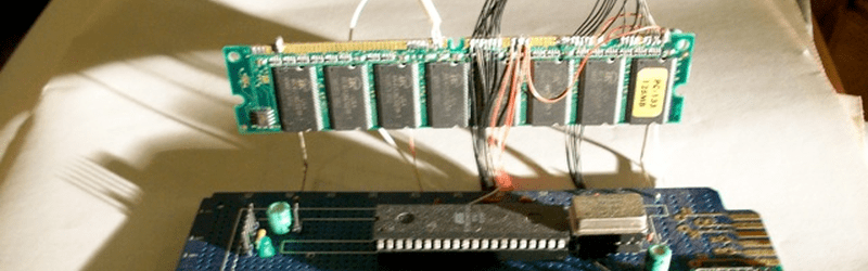
The answer lies in the selection of components. The analyzer uses a 128MB SDRAM DIMM (like an older PC might use for main memory). That makes sense; the Arduino can’t store much data internally. However, it isn’t the storage capacity that makes this choice critical. It seems [esot.eric] has a way to make the RAM “free run”.
The idea is to use the Arduino (or other host microcontroller) to set up the memory. Some of the memory’s output bits feedback to the address and data lines. Then the microcontroller steps aside and the SDRAM clocks samples into its memory by itself at the prevailing clock rate for the memory.
Of course, this isn’t good for things like complex triggering, and you give up some memory storage to the control “program” (if that’s the right word). However, it is easy to see this technique being useful in other cases where you want to offload the CPU for repetitive data transfer. For example, [esot.eric] has also used this method to drive an LCD panel.
Just to prove the point, the video below shows the device working even after the AVR microcontroller is removed. It is only necessary during the setup phase. Admittedly, the logic analyzer part isn’t the cool part. If you want a logic analyzer, pick up a DSLogic from the Hackaday store or one of the many other inexpensive ones out there. If you want to roll your own, there are plenty of options for that, too.
But for sheer audacity and dirty trickery, you have to admire how this design uses an SDRAM in a unique way. It makes you wonder what other components we could use in strange ways.


The old Atari Asteroids arcade game used a similar trick to rotate and move the asteroids around since the CPU was a tad anemic (1MHz 6502 if memory serves me right).
Part of the data out from the memory was fed back to itself and the remaining data went through DA-converrters that controlled an X-Y-Z display. We used to run the game on our oscilloscope when we where diagnosing it and playing on a 4.5″ display isn’t the easiest. :)
I haven’t even had a beer yet today and I want to say “I love you, man!”. I spent a large number of hours in front of that wonderfully crisp vector display of Asteroids.
Program a truth tables into the RAM…now you have a poor man’s FPGA.
This project is really clever and fascinating. I like the idea of reusing those old sticks of SDRAM I have laying around.
Your comment reminded me of something I’ve done at home on numerous occasions…
In a pinch I’ve used a Terasic DE1 FPGA development board and Altera’s SignalTap logic analyzer software. It’s possible to pick any of the pins (70+ on the DE1, IIRC) on the I/O headers to be the clock source and the remainder as inputs. Setting up a sample clock using one of the on-board oscillators is very easy, too. Since SignalTap is designed for such things, it has all the abilities to set up complex triggers. The only real drawback is that the FPGA project needs to be recompiled when complex triggers are changed or added. Basic triggers (rising/falling edge, high, low, etc.) are configurable on-the-fly.
The sample depth is ultimately limited by on-chip memory resources. Larger FPGAs available on other development boards will have more resources, obviously.
If you’re willing to write some VHDL/Verilog, the sky is the limit on custom, multi-tiered triggering options and it becomes easy to set up a data generator/testbench for testing other equipment. In other words, just as an example, [esot.eric] could use an FPGA development board to feed his new logic analyzer to ensure everything was working well.
FPGAs… As I understand (and I don’t, really): Many can actually work directly with SDRAM (and DDR, etc.) with built-in controllers for the purpose, others can be (manually) programmed to. Once a (fast-enough) FPGA’s in the picture, there’s really no need for “Free-Running,” as the FPGA itself should be more than capable of handling proper timing of back-to-back burst-read/write instructions… And… would certainly be a more-reasonable route to go for most product-designs.
It’s interesting that Altera makes software for using FPGAs for that purpose… Something I’ll definitely keep in mind when/if I ever get into FPGAs. Thanks for that insight!
Complex triggers… now that’s something I hadn’t really thought about… sdramThing may be going the route of “sdramThingZero” in the not-too-distant future… ( https://hackaday.io/project/10119-sdramthingzero-133mss-32-bit-logic-analyzer ). This guy would get rid of the AVR altogether, and be more of a peripheral to be added to devices like Raspberri Pis. Ridiculous as it may sound, it makes some amount of sense, since the Pi’s GPIOs are comparatively slow (and limited in numbers). I mention this because: Since Free-Running is necessary in this setup, complex-triggering is something that would seem difficult… without adding some sort of dedicated controller/FPGA/CPLD for the task. Hmmm…. You definitely have me thinking… Check out that page, I’ll probably be adding some logs on that thought-process in the future… Thanks for that!
For a serial-pattern, I can *vaguely* visualize something with an XOR, and a state-machine sort of thing within the Free-Running mode, where it outputs the bit it’s looking for, jumping back on itself until it’s detected… when detected, the XOR-output would go zero, which would bypass the jump-back-address with a jump-forward…. I think it’s possible. This’d be somewhat limited, something like: the (serial) pattern to be detected must be slower than 1/8th the sample-rate (due to burst-lengths and the number of instructions necessary to jump) and the rate of the trigger-source must be known(?). And, then, if you’re looking for a pattern of multiple parallel data-bits, more logic would be necessitated. Maybe a binary-comparator… Might, actually, only take a small handful of additional logic, hmmmm…. (although, implementing this in Free-Running mode would pretty much eliminate the ability for a circular pre-buffer… right? Hmmmmmm….)
Again, thanks for the thought-point, complex-triggering kinda makes-or-breaks the usefulness of a logic-analyzer.
You are exactly correct… FPGAs to have the capability to interface directly with SRAMs, DDRs, RLDRAMs, etc., but I’m not sure that could be used with SignalTap.
To clarify a little, the SignalTap software is really intended to be a logic analyzer for signals internal to the chip. For example, if you’re troubleshooting, let’s say Ethernet packet processing, you can use SignalTap to look at signals between VHDL/Verilog blocks to help pinpoint issues. The alternative to this would be to route the signals you want to observe to external headers on a board and use a dedicated logic analyzer. This is a pain compared to having the baked-in solution Altera provides.
Also, I was using their software outside the normal use-case. It works very well when used as a general-purpose logic analyzer even when you’re only looking at external (not internal to the FPGA) signals.. I’m familiar with the interface/controls from the FPGA development I do at work, so that’s why I immediately identified this as the quickest option for what I was trying to accomplish.
Unfortunately, I don’t believe there are any provisions for using off-chip (SRAM, DDR, etc.) RAMs for capturing samples with SignalTap. Therefore you’re limited to your on-chip memory resources (M9K, M10K, etc.).
Touching on your “serial-pattern” statement, doing such a thing in an FPGA would be as easy as writing code to generate a shift register the length of the pattern you were trying to find and comparing that against a register that contained the pattern. As data shifted through, it a match were found, a flag could be set. That flag could be used to trigger SignalTap.
Again, touching on the “serial-pattern” statement… if, for example, you wanted to look at a serial stream from a UART, but wanted to trigger on a particular byte, all that would be necessary is to write VHDL/Verilog that would deserialize the data, compare, and trigger on a match. The sky really is the limit with FPGAs.
Ahhh, I get it! SignalTap is basically exactly what it’s called… it shows you the (generally internal) signals, an *internal*-logic analyzer… In the microcontroller-sense it’s like a debugger looking at the internal-registers. And what you did was route external signals to internal signals to create an [external] logic analyzer. Similar, again, to using a microcontroller-debugger to watch the PORT registers. Turning a debugger into a logic-analyzer. That’s pretty durn clever. Props!
Yep Yep! It’s easier with SRAM, since the address-lines are pretty much linear (whereas an SDRAM’s address lines are written twice, once for the row, and once for the column, as well as the necessity to open/close pages). The address-lines on an SRAM are basically the inputs to your “FPGA”, the data-bits (once the truth-table’s been written) are the FPGA outputs.
As far as sdramThing, you’re on to something, here, as well…
“Free-Running” can be combined with a tiny bit of logic/multiplexing to handle things like jump-rerouting based on an input… So, e.g. you have a loop that jumps back on itself until a certain condition is met… at which point the multiplexer switches, forcing it to jump somewhere else. In that sense, it’s a bit more like a a really long switch() statement.
As far as SDRAM itself… I hadn’t really thought of it… you could have a certain page open already, then a single “read” instruction would act just like the SRAM example, earlier. Hmm… And, on top of that, you could open an entirely different page for the shear purpose of having different truth tables to look through. Interesting. It would take a little bit of set-up to switch those pages, but not a whole lot, really.
I have a vague thought of storing a table of sine-wave values… The address inputs to the “FPGA” would be, essentially the angle requested… the outputs would be the sine-value. BUT, e.g. switching to the next “page” would load up another truth table which could essentially give a phase-shifted output… e.g. sine(angle + 1).
In the SRAM example, earlier, this’d be kinda the equivalent of having two SRAMs in parallel with separate (addressable) Chip-Select inputs.
Intriguing.
Further, still, there’s the possibility to *combine* your row-activation and column-access addresses… I did this early-on since the microcontroller was too slow to switch around all the address bits between a row-activation command/instruction and a column-access (read/write) instruction…
E.G. in Row-Zero, all *column* addresses are where you’d expect them. (The first *column* of *your* data is at address 0). But, in Row-One, all column addresses are offset by one; the first column of *your* data is located at address 1. And so-on. (And, it’d wrap).
The reason being, again, that your address-inputs, then, needn’t be changed between a row-activation instruction and a column-access (read) instruction… This’d give a MUCH LARGER table… each *page* is only 512/1024 columns (e.g. A9:0 are paid-attention-to in a column-read access, kinda like having 10 inputs on your FPGA/Truth-table), but there are *thousands* of *rows* (e.g. A11:0 are paid-attention-to in a row-activation).
Got me thinking, yo!
Program this one into it and you have a universal Turing machine.
0000
0011
0101
0111
1000
1011
1101
1110
But it may take a bit of work coding an emulator “tape” for it before you can boot Linux on it….
could you clarify your statement? what does the row index represent, and what does the column index represent? etc?
http://mathworld.wolfram.com/Rule110.html
Wow, I tried, but that’s just too… something… for me to grasp. Care to explain for the lay-man?
Oh you mean something metaphoric? OK.
A sufficiently large sheep will provide enough wool to knit a full body suit for a brontosaurus.
There does that make things clearer? No?
Try this then, https://en.wikipedia.org/wiki/Rule_110 and this http://www.complex-systems.com/pdf/15-1-1.pdf
Guess it’s just outta my league… Even wikipedia’s explanation contained too many links I needed to click-through before I could understand what it was saying. Sounds interesting, though.
@esot.eric: Imagine a pixel on your computer screen. It POTENTIALLY has a neighbor above, below, to the left and to the right of it. The rulesets, like 110, just tell the program how to build new pixels based on the pattern of neighbors surrounding it.
More like a finite state machine than an FPGA, but,,,,
Holy shit. A real hack on Hack-A-Day!?
Don’t worry. I’m sure someone in quality control will make sure it never happens again.
Pretty sure QA was already there with the *tremendously* useful link to the HaD store :)
HAHAHA AK47RFa, you right, very useful link.
My thoughts exactly.
It makes a nice change. Excellent post. Hopefully more to come this year.
Exactly. This is the kind of articles I would like to read MUCH more often here.
Hey… Thanks, all! :)
$title=~s/dirty/clever/
>Program a truth tables into the RAM…now you have a poor man’s FPGA.
This sounds quite interesting!
isn’t this called a state machine?
Yeah, but we don’t have to burst his bubble…
no bubble burst, here… though, curiosity peaked. Please explain.
You mean “piqued” of course…
plateaued?
memory feedback based state machine
http://ruemohr.org/~ircjunk/tutorials/elex/fsmflash/main.html
AWESOME!
That is a 11/10 for hackishness.
Ray Moore: re: “isn’t this called a state-machine?”
Not trying to give you the brush-off, infact I wrote up some thoughts on the various state-machines in sdramThing, and SDRAM, feel free to message me if you’re interested, though it might be a bit dense.
Problem is, the ol’ “State-Machine” **definition** is something I didn’t really grasp in my studies… It seems to me like, at the basic level, nearly *everything* digital is a state-machine. Even something so simple as a single variable, or single byte in memory, is a state-machine… It has a state, its value. Its state can be changed by writing another value… Its state can be incremented, by adding 1, etc… Then there’s a “bigger” state-machine that is responsible for doing whatever is to be done to that variable’s state… Say incrementing, or decrementing, if it’s a counter. Then you can go from there and say that the Processor (CPU) has states of its own which controls the state of the thing being done to that variable’s state. The CPU, depending on its state, chooses whether to use the “counter” state, or the “addition” state, or the “subtraction” or “copy”, or many others… Then, of course, the CPU runs an application (or gazillions of them, each of) which has states of its own… So, then it’s a matter of what level of state-machine are we talking about…? Oh, we could go further down the “smaller-state-machine” path and look at that variable as a combination of bits, each of which has states of their own… So the 8-bit variable has 256 states of its own, and each of the 8-bits within the variable has 2 states of their own…
So, I guess the question is… “isn’t *what* called a state-machine?”
Call me an id.10.t, but where did you find or learn the pinout for the sdram?
Could this possibly be used for increasing the ram for uC projects that run out of ram? I mean instead of needing an ATmega2560 for a project, use a 328 and this?
For the SDRAM Chips you can look at the datasheets from Micron, they include pinouts and functional details. My go-to datasheet is that from the MT48LC8M8A2, not that I actually have any DIMMs with it on-board.
For the SDRAM DIMM pinouts, there’s Intel’s PC SDRAM UNBUFFERED DIMM SPECIFICATION Rev 1.0.
Sure, SDRAM could be added for increasing uC RAM, but accessing it is a bit more difficult than just a memory-read instruction. Doing it with this “Free-Running” setup is a bit overkill, however, unless you need that functionality, specifically. Some AVRs have an external-memory *interface* (e.g. ATmega8515), which might, still, be difficult to use with S*D*RAM, but adding *SRAM* is an easyish step which also allows for using the regular-ol’ memory-read/write instructions (I don’t, however, know how to tell the compiler that that extra memory is available…).
Some one has already interfaced and written code for an AVR (ATmega88) to interface to an SDRAM. Here is the link: http://spritesmods.com/?art=avrcpm
Was unaware of that one, thanks! SpritesMods are generally quite impressive. Unless I missed something in my brief overview, this one is actually using a DRAM, rather’n an SDRAM, but I think the concepts are quite similar, and much of that code could probably be used for SDRAM.
On that note, I’ll point out one that I found particularly inspiring early-on…
http://tinyvga.com/avr-sdram-vga
This guy uses the same “Burst” mode, of a single page, as the timing-controller for scanning a row of pixels. Then another burst is set-up for the second row (of pixels), and so-on.
I’m sure there are others hacking SDRAMs into their AVR projects, probably PIC, and others as well. One of the nice things, I’ve found, is that even though they’re rated for speeds way-faster than an AVR, they appear more than capable of running at *much* slower speeds, reducing the barrier-to-entry quite a bit, as opposed to, say, DDR (which allegedly can’t run at less than 85MHz).
Yes, the AVR-CPM project uses DRAM but since SDRAM is “Synchronized” DRAM, which means that the DRAM is synchronized to the CPU’s clock. SDRAM could be used as well on his project but the parts this particular inventor chose are available for a few dollars each and come in leaded through hole DIP or ZIP packages, which makes for easy build and interfacing (they are not SMT).
With the exception of the clocks and the DQM pins, there is not much difference between the DRAM and SDRAM.
I’ve seen the TinyVGA you posted. Its a nice hack but in my opinion, it would be easier to interface with an graphic LCD instead … but then the TinyVGA would not be a hack, eh? LOL
Interesting. I’m going about it a bit backwards, having a pretty-durn-good understanding of SDRAM, but nearly-ziltch of DRAM. Just looked up the datasheet of the DRAM used in AVR-CPM, and indeed it does look quite similar, in interface, to SDRAM. There are definitely differences, though, with SDRAM’s having some internal configuration registers, multiple open banks, and burst-modes… Also, SDRAM is filled with “pages” in “banks”, so whereas DRAM appears to be a two-dimensional array, SDRAM is 3-dimensional. Also, some SDRAM instructions can’t be executed more than once (in other words, the /CS line can only be active, for those instructions, during *one* clock-cycle). Interestingly, it appears that DRAM’s “refresh command” is, essentially, nothing more than opening a row and closing it, whereas SDRAM has explicit commands for doing-so… And here I thought I came up with something unusual by refreshing via opening/closing a page ;)
All that said, it does look like DRAM is quite a bit easier to interface than I originally thought. It’s basically not much different to work with than, say, an SRAM/EPROM… Just select the row first, then treat the “column” like a regular-ol’ SRAM/EPROM access. (And remember to access all the rows often-enough to keep it refreshed). Cool.
TinyVGA -> LCD still seems like a decent hack, to me… Unlike a GPU/vid-card, where there’s a dedicated processor for addressing, timing, and routing the memory-data to the actual pixel-data-output, TinyVGA uses the SDRAM’s internal clocking-mechanisms to do all that…
Some microcontrollers support direct addressing from external memory. The FMC memory controller of an STM32F429 can run code from external sdram.
Or even better from QSPI, but I guess only for FLASH and just reading.
My man, Al! Thanks for the write-up!
This’s been a long-running project, revisited several times over the past 4-5 years. You can tell in the video I’m a bit long-winded on the matter. Great write-up, thanks!
Speaking of long-windedness, here’s a timeline for the video, put together by a buddy of mine over at .io, who I can’t thank enough for all his enthusiasm on this project, and for convincing me to put this video together. https://hackaday.io/hacker/1724 Yo, Frankstripod! Where you at?
0 to 1:30 Description Free Running RAM
1:30 Start Loading SDRAM commands
2:55 Component Overview
7:20 Data Refresh Starts
8:50 Reset AVR, Free Running
9:40 Remove AVR!
11:00 Bonus sample mode switching!
22:10 Better sample while Free Running
I’d been meaning to make a snappier vid, but never got around to it.
Great job esot.eric, keep on hacking!
Very interesting. Didn’t know that was possible.
This is a very cool hack. I remember building a memory tester way back when that auto-clocked the memory. But this is much cooler! ;-)
So how do you measure the access speed of an EPROM with scarcely more than a wristwatch back in the eighties…? You burn an auto-clocking pattern into it, pipe the same signal into a cascade of TTL 490 decade counters you just happened to have laying around then time whatever comes out on the other end with an LED and your wristwatch at a leisurely pace. Ehhh, kids these days have it way too easy… (now get off my lawn, etc.)
… Depending on how fast the microcontroller is, these projects range from adequate to not very useful.
Almost everybody surely knows the Cypress CY7C68013-56PVC by now?
http://sigrok.org/wiki/Lcsoft_Mini_Board
These work pretty good with sample rates up to a few MHz which is plenty for all arduino and lots of other microcontroller stuff. (serial, I2C, isp etc).
Pulseview & Sigrok have been improving steadily over the years and now support 25+ different protocols and can interpret the data for a lot (30+) of popular “hobby” ic’s
But I’m diverging.
Keep it up, really nice hack.
They (sigrok) even fixed the bug recently, which prevented the Cypress FX2 based LAs from reading at the speediest rates. The only problem with some of them are the 74HC245 buffer chips, which are powered from 3,3V and the device promised 5V input tolerance, which according to datasheet is not allowed. Quick fix is to put a switch to select the input voltage for the HC245 and as such the input voltage of the signals.
Looks like a useful tool, thanks! Maybe I can bypass writing my own GUI, if I ever get that far :)
Nice fix for the HC245… Always wondered what techniques professional LA’s use for thresholding… CMOS, TTL, LVTTL, LVCMOS, so many options, so many different threshold-values… And what when floating…?
For the non-floating case, I suppose one option would be something like an AHC244/5 with an adjustable power-supply (again, great idea, thanks!)… fed into another at 3.3V. 5V tolerant inputs, and, then, one could almost set any threshold value by varying its power-supply… Maybe run it off 2.5V-ish for testing TTL-level signals.
Another idea may be to use two (or more) channels per input, with differently-powered AHCs, then one could get various analog-ish values. and/or notice of when a value is neither technically high or low. Might take some characterization-testing.
Oh, and if already throwing buffers at the inputs, another option might be two latches (AHC574?) per input, which could be configured for opposing clock-edges and write to parallel bits… A sort of “poor man’s” DDR-input, double that sample-rate without necessitating a dedicated DDR-controller.
So many ideas inspired by y’all!
If any of you take any of these things on, please link ’em here!
I wish i knew what tricks they use, but another fix (also not mine, like the switch fix) is to use a 74LCX245 instead, which can be powered from 3.3V and still have 5V tolerant inputs. It’s just a little hard to exchange.
I was thinking of using FETs, like the sparkfun (bidirectional) level converter uses BSS138. Only i have an 8 channel version with double FETs, so it doesn’t matter which side has the lower voltage (that’s not a huge problem with single FET version, just turn it around, if input signals are less than what’s fed to the HC245). I just don’t know if it’s fast enough, but atleast if i need more than 5V tolerant inputs, i probably don’t need that much speed anyway. If switch mod or LCX mod is not done, then it would require the FET mod for 5V also.
My LA is different looking than what Paul linked, but basically the same (only 8 digital channels)
http://sigrok.org/wiki/MCU123_Saleae_Logic_clone
For the FET mod, it’ll require one of the GND pins to be modified as voltage output (the same voltage as goes to the HC245).
But on to the topic, that’s some wicked thinking. And sigrok is great, no need to build your own full GUI.
Good idea, but wrong parts Several issues with using discrete MOSFET for level translation. Their threshold is very loosely spec, so you’ll have hard time going for lower voltage. Their high gate capacitance that loads your D.U.T. which limits speeds and affect the actual timing.
That’s what they use for the earlier level translation device except that they are on the same chip so their threshold characteristic matches and they use feedback to feed threshold. The smaller geometry means smaller capacitance and they come with ESD protection.
This application requires a unidirectional translation, so just get the proper level translation transceiver chips with dual supplies..
As for professional designs, they use high speed comparators so that they can tweak the threshold voltages. Unlike the $10 logic anayzer, they also have series resistors and compensation network in there to reduce the loading on DUT but still maintain the timing.
The guy lives up to his name, awesome project!
Right-on, thanks! Cool Gameboy->VGA converter, BTW: https://ackspace.nl/wiki/Gameboy_VGA_adapter
I used to do something similar with eproms, you could setup a poor-mans PLD/GAL/PAL if you needed a quick and dirty way to combine all your “glue” logic. Determine all the addresses to generate the correct truth table, and write the desired output values to those addresses. You could even feed output back into the address lines to make flip-flops and the like.
Exactly this way (EPROM, 555 and shift registers) I created an animated LED array sign back in the 80’s. Writing the “program” for the animation using just graph paper and pencil was excruciating experience.
I started to think about how this could be possible, and then I read that SDRAM uses a fairly complex finite state machine with its own internal registers for internal control of reads and writes. He’s found a way to leverage this internal state machine to emulate the operation of a logic analyzer, and it runs independently of the host microcontroller.
That is actually really cool sir!. I often though how I could (re)-use my buckets of old computer ram with an avr for storage. Nice to know someone else thought of this and beat me too it.
Nicely done!
Useful comments – I was enlightened by the points ! Does anyone know where I could obtain a sample a form copy to use ?