
To a lot of people, radio-frequency (RF) design is black magic. Even if you’ve built a number of RF projects, and worked your way through the low-lying gotchas, you’ve probably still got a healthy respect for the gremlins lying in wait around every dimly-lit corner. Well, [Michael Ossmann] gave a super workshop at the Hackaday Superconference to give you a guided tour of the better-illuminated spaces in RF design.
 [Michael] is a hacker-designer, and his insights into RF circuit design are hard-won, by making stuff. The HackRF One is probably his most famous (and complex) project, but he’s also designed and built a number of simpler RF devices. And the main point of his talk is that there’s a large range of interesting projects that are possible without getting yourself into the fringes of RF design (which require expensive test equipment, serious modelling, or a Ph.D. in electro-wavey-things).
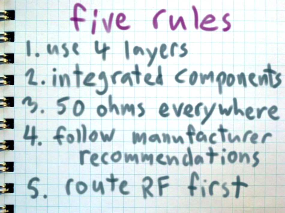
You should watch [Mike]’s workshop which is embedded below. That said, here’s the spoilers. [Mike] suggests five rules that’ll keep your RF design on the green, rather than off in the rough.
1. Use Four Layers
Four-layer PCB prices have gone way down, and having unbroken power planes on the inside of your board makes your design simpler and makes for a consistent RF environment throughout. You could build it on a two-layer board, but then when it doesn’t work, you’re going to need that pricey test equipment. Keeping the layout simple, with RF traces all on top and power planes in the middle, is insurance against the gremlins.
2. Use the Most Integrated Component Possible
Design your board around the most-integrated parts you can find. That’s going to mean picking an integrated transceiver IC that’s got everything in silicon. That’s a whole lot of tricky design work that you won’t have to do. The same applies to filters; you could spend hours designing a fancy filter and layout, or you could just find the right part ([Mike] likes SAW filters a lot) that fits your design.
3. Design for 50 ohms Everywhere
Impedance matching: you just can’t get around it. Most manufacturers’ parts are built for 50 ohm inputs and outputs, though, so there’s no work for you to do there. Your only job is to make sure that the traces between the parts have a 50 ohm characteristic impedance. How do you do it? KiCad has a tool, and otherwise there’s the Internet. You just need to know some properties of your PCB from the manufacturer, plug them into a calculator, and then you get out a trace width that will give you 50 ohms across the board. Remember that unbroken power-plane in the second layer of your four-layer layup? It makes the same trace width work everywhere. That’s the hardest part of RF design, done.
4. Follow Manufacturer Recommendations
What if you absolutely need to use a part that doesn’t work on a 50-ohm standard? Unless they don’t want your business, the manufacturer will provide you with a reference circuit that transforms the output to 50 ohms. Your job is to take advantage of the work of their applications engineers. There will often be a layout specified, sometimes even down to the part numbers. If they tell you how to get their chip’s input or output to work with a 50 ohm single-ended transmission line, you do it.
5. Route the RF Parts First
The RF signals are the most sensitive part of your circuit design. We already know what the desired RF trace width is, so all that’s left is laying them out. [Mike] advises you to keep the traces short, relative to the frequency of interest. After you’ve laid our your RF signals, keep your digital traces a little bit away from the RF traces whenever possible. That’s it.
Examples
In the second half of the talk, [Mike] walks through a number of his RF designs and demonstrates how he applied the simple five rules to build some interesting devices. Reference designs, short traces, and integrated parts abound. He wasn’t joking. In some of the devices, “the RF section was the easiest to lay out — I just copied it from the data sheets!”
We’re not going to work through his examples. We wouldn’t do them justice, and there are just a ton of RF design tidbits. You’re just going to need to watch the video. Enjoy!


I didn’t get a chance to sit in on this workshop, the thing sold out immediately (you should have seen the line for overflow seating). I’m so glad to have this recording online. Thanks Mike Ossmann!
Can anyone give an example of a calculator and how to use it? I have found 3 or so but not sure on values.. i want to know approx how wide my trace should be for 50 ohm.. assume 2 layer 0.8mm thick pcb and 1oz copper.. can someone just give a good enough answer? I have used 0.4mm which worked ok but I just guessed that.. I would have thought this was a common question yet googling returns nothing definite!
try this:
http://wcalc.sourceforge.net/cgi-wcalc.html
also Saturn PCB toolkit is a great tool fore more than just rf:
http://www.saturnpcb.com/pcb_toolkit.htm
I have used both in several designs.
This is a good one:
http://wcalc.sourceforge.net/cgi-wcalc.html
Saturn PCB Toolkit is a great one too:
http://www.saturnpcb.com/pcb_toolkit.htm
This is also a useful tool specific to rf and you will need to study up a bit to understand how to properly use it:
http://iowahills.com/9SmithChartPage.html
I have used all of the above on several designs and they have given good results
The calculator of my layout program says: Around 1.5mm would be the right value. +/- some 1/100mm for Er (4.0 to 4.4) and track thickness.
I remember to have used 1.5mm on 1,6mm 2 layer PCB. As the dielectric height and therefore the track width goes down, the influence of the copper thickness increases.
Your 0,4mm track gives an impedance of 95 Ohms. Not exactly what you want.
Here’s one I’ve used:
http://emclab.mst.edu/pcbtlc2/
Just a quick note: in general, those rules will get you about 70% of the way there. The remaining 30% is the “total black magic” stuff. And if you’re using commercial ICs, and not doing precision measurement stuff, you’ve got plenty of margin to work with 70%.
Just as an example, if you look at the “YARD Stick One” right there, the SMA connector that’s on the end? The ‘example footprint’ that you’re given is typically for a 2-layer board, signal on top, ground on the bottom. Typically nothing in the datasheet tells you this. If you do it on a 4 layer board, the signal is now way closer to the ground plane, so you’ve got a lot of excess capacitance there. The impedance of that transition is typically around 15-20 ohms or so.
So if you have the connector a fair amount away from the first component (~multiple wavelengths), you’ll probably lose around ~1/3 of your signal power just getting on the board (S11 is typically around -5 dB). But that’s only 1.5 dB loss. Not a big deal – you can probably absorb it. But the connector datasheet’s quoting “below 0.1 dB insertion loss”, and you end up with 1.5 dB, even though you followed everyone’s recommendations.
How would you recover that 1.5 dB? Moving a component right beside the connector gets you most of the way there. The best fix is actually to clear the inner planes underneath the connector, make a solid ground plane on the bottom and stitch it a ways in. Which is quite a bit more work. Like I said – simple rules get you ~70% of the way there.
(Altera has a neat app note here showcasing the effects. Note that their SMA measurements are with a component nearby, which minimizes the effect at low frequency).
That’s one neat app note. You wouldn’t happen to have any more of those neat things up your sleeve, would you? ;)
Most of my stuff is with HF (<100MHz) and my SMA connectors are edge-mounted.
Even so, I reckon a re-draw of my KICAD SMA component is on the cards, to be on the safe side.
Truth. The center pin land presents a gigantic capacitive discontinuity if the groundplane is left intact. The best bet is to get a connector with a center pin smaller in diameter than the microstrip width in your application, but that’s often not feasible. That means inner-layer plane relief. You wouldn’t believe how much pain the pros go through tuning connector transitions. It’s insane. Another discontinuity: edge-of-board plane relief. Believe it or not, that 10 mil or so that all PCB vendors require to prevent delam and moisture incursion leads to an inductive discontinuity where the center pin is hanging out over bare substrate for some length. (It can be seen clearly in the YARD Stick One photo as the light green band surrounding the board) Tuning out that discontinuity with proper plane relief can mean the difference between 12-15 dB return loss and 25+ dB at 2.4 GHz.
Read the book SECRETS OF RF DESIGN. Most impedance matching is done with a VNA which is $$$$ but low cost versions are being sold in QST magazine.
It’s been my experience that trying to calculate and lay down your own 50 ohm traces will get you close-ish, but the pcb fab can do a better job because they know their processes. Note all my RF designs are six layers, with a ground layer on either side of the 50 ohm layer, and every trace on that layer is 50 ohms, so I have a different design system than the article, but when I do a board, I do all the 50 ohm layer traces 10 mils wide and then tell the fab house that they can do whatever they want with trace width and adjacent interlayer spacing thickness to make 50 ohms. The fab house I’m using currently sends me a test specimen with each board, cut from the same stackup, that has 50 ohm traces running through it, and decorated as a ruler, allowing me to test their work, use it as a ruler, and also advertise their services to anyone who sees it. That’s fancy, of course, but I think any good board house can, should, and will do a better job of trace width than 95% of pcb layout people.
What house do you use?
Well I break most of the rules.
I use double sided PCB but leave one side complete (no etching at all) as a ground plane. The only pin though is for grounding, everything else is surface.
The etched side is a poured plane (minimum etch) with big spacing for RF paths to that the signal isn’t effected by parasitic capacitance.
The the whole thing goes into a metal box. Sometimes you need a box or on the PCB as well.
And … more discrete parts. More fun this way.
RÖB does it how anyone with experience does modular design (or reads ARRL publications). It can get noisy if the ground layer is too close to the signal path in VHF, and few people understand why shielding has air-space between it and the board. The 4 layer rule is BS, and putting a solder mask over the signal path is bad practice too. If people don’t understand why — than ask the thousands of RF guys who do know.
Also, the reason people use 45′ traces with a specific wavelength ratio clip is very important at higher frequencies, and is not even the ideal method. However, in low frequency design people should still follow the same microstrip & stripline design rules out of habit.
While this is a charismatic lecture, most people should only take away the advice of reading manufactures app notes.
Been doing RF design since the late 80’s. These rules are a good start, but there is no substitute for experience. If you don’t have it, ask a grizzled, bearded RF engineer near you.
Yup.
“The Dunning–Kruger effect is a cognitive bias in which relatively unskilled persons suffer illusory superiority, mistakenly assessing their ability to be much higher than it really is.”
:)
“To a lot of people, radio-frequency (RF) design is black magic. ”
Yes it is and will be. It cannot be done properly without measurements and many prototypes.
Amen brother! Been doing Ku band and under for 22 years, now moving to W band.
I know an RF engineer – she doesn’t have a beard.
She isn’t grizzled either, as far as I can tell (no grey that I know of).
One question I would like answered in a simple way is…
What is so ‘perfect’ about 50 ohms. Is it just a standard? or is it the perfect balance of current and voltage for some reason?
I know that free space has an impedance of 376.720 313 461 77… Ohms (thanks WIkipedia!) – wouldn’t a higher impedance be easier to couple to free space?
Is it like that tail that size of the shuttle’s boosters being decided by the width of a horse’s bottom due to the transport infrastructure?
I found this “The most common story is that 50-ohm high power coaxial lines were first made using standard sizes of copper pipe, such as 3/4 inch for the inner conductor and 2 inch for the outer conductor”. I wonder if it is true….
I’ve heard things about impedance of a dipole being ~75 ohms, and something else being ~25, which made 50 a good compromise.
Mike actually mentions it in his talk — and says that he’s heard a bunch of these stories and doesn’t believe any of them. I think that’s probably about right.
The most believable I have found is that coax around 30 Ohms gives the most power transfer for any given cable diameter, and around 75 ohms gives the lowest loss for any given diameter of cable, so the mid-point of 50 Ohms became the standard.
It sort of follows that where loss is important (signal distribution networks, long cable runs) 75 ohm coax is used (e.g. TV). Where power transfer is also important (e.g. RF transceivers) 50 Ohms is used…
I used to work at a 15kW AM transmitter site. The feedout to the Antenna’s (called aerial feed) was a wire that was at the center of four other equally spaced wires suspended along poles which have various stages of insulators in the structure. The transmission voltage (in the kV range) was far too high to use anything like cable.
The aerial feedout was about 318 Ohms and there was an impedance matcher at the base of the antenna. The matcher consisted of a coil and an air gap capacitor that were about 200kg each.
Different antenna configurations have different characteristic impatiences and best practice is to match these impedance with both the cable and output stage but that is not always practical so often a tuned circuit is used to match the system.
It’s a standard. Like the PL-528 and the RG-58U coax. Most ham antennas are 50 Ohm. A folded dipole is 75 Ohm (from memory but not sure).
If you were designing old terrestrial TV systems then you would target 75 Ohms as that is what the cable and antennas are for TV. Well actually the antennas are 300 Ohm but they have a balun.
I think the folded dipole is around 240 Ohm.
http://www.microwaves101.com/encyclopedias/why-fifty-ohms
Scott Gilmour is one of the few remaining guys out there that really know microwave inside and out. especially microwave tubes. He can put it in terms that mere mortals can understand too.
As i heard it, the first koaxial cables was made by putting porcelin/bakelite beads on a single wire and then putting a shild braid on the outside, for use in the high freq radars in airplanes, but the copper pipes would have worked in other installations.
A quarter wawe dipole is around 75ohm, unless you make it V shaped, then you get close to 50, a GP is around 50 on a decent groundplane as a car body and can be tweaked with the angle of the groundplane rods if used stand alone.
Many other antenna designs are supposed to be used with ladderline or open feeder lines and a matchbox, but those marchboxes are usually fed with a 50 ohm input.
I thought coax for aircraft radar was one of the first uses of teflon as a dielectric.
75 Ohms = open dipole, 300 Ohms = closed dipole, ~36 Ohms = Marconi antenna. Air mounted Marconi antenna would use wires as a ground plane (instead of real ground connection), whose angle and length could often be adjusted to get close to 50 Ohms. So there you have it, 50 Ohms is a fair compromise to both common dipole and Marconi.
And for the closed dipole you will have to use a balun anyway.
True.
I have an extra Hack RF SDR from Mike Ossman. If interested, let me know.
How much and where would you ship from?
Destination would be CZ, Central Europe…
Can I get one HackRF one from Mike Ossman now? What is the procedure?
Just order one. No tricks involved.
Has anyone tried making 50ohm traces using the OSHpark fab PCBs? How close is it to 50ohms?
Sorry. My bad. Commented before watching the video.
Perhaps the most important and overlooked topic is the current return path; every trace carrying a current has an associated path that returns the current to it’s source.
This path is always the path of least impedance, which for ~1MHz signals translates to the path of least inductance.
The path of least inductance for a trace is parallel directly beneath it on the adjacent power/gnd plane which is the main reason why split planes are the bane of RF; a split plane underneath a trace greatly increases the inductance as the current return path has to move away from under the trace to ‘find’ an alternate route.
This can cause all sorts of fun such as ground bounce, signal ringing/overshoot/undershoot, sometimes the alternate route happens to be another signal trace..
Ground bounce is an alternating voltage potential across your ground plane which causes voltages on signal traces to appear lower or higher depending on which part of the ground you are referencing to and at what time.
It results from the change of magnetic flux and the inductance of your trace; the faster the rise and fall time of your signal and the higher the inductance the more ground bounce you’ll encounter.
Digital circuits generally don’t mind ground bounce because a small deviation on the signal trace still translates to either a ‘0’ or a ‘1’ but analog circuits on the other hand are heavily reliant on the voltage of a trace at any given time and cannot tolerate such deviations.
I firmly believe that splitting your ground plane to divide digital and analog circuitry is a bad strategy to stop ‘high frequency noise leaking into your analog circuitry’ because it does not take into account WHY it’s happening and could potentially increase the impedance of your traces because your current return path is being neglected thus making things WORSE.
Instead I suggest that you focus on keeping the current return paths of > ~1 MHz signals out of the way of analog circuitry to ensure that the ensuing ground bounce does not create a voltage potential across the analog section of the ground plane and to keep your ground plane whole to ensure that your trace inductance stays at a minimum which reduces ground bounce.
Signal ringing / overshoot / undershoot are deformities that appear on your square wave if your signal encounters different impedances, takes up a significant portion of the wave length of the frequency of your signal (though typically for square waves we tend to refer to rise and fall times to determine the threshold) and does not have a terminating resistor.
They are the result of not treating your trace as a transmission line and can be detrimental to your signals which can cause some of the following behaviour: false clock/data, missing clock/data and in the worst case destroying components
(e.g. ICs, FETs, etc.) because the voltages are too high / low for the specs.
Analog devices has a white paper(MT-097) which has a nice rule of thumb to determine whether you should treat a trace as a transmission line and use termination:
Multiply the rise/fall in nanoseconds by 2, this is your max trace length in inches before you need to treat it as a transmission line.
Which brings me to the next relevant topic; decoupling caps.
As we have seen the current return path is important in ensuring the quality of your signals and keeping your ground plane quiet and decoupling caps play a significant role in this; decoupling caps decrease the size of your current return loops which decreases inductance and can improve ground bounce and signal degradation problems.
Every current wants to return to it’s source and without decoupling caps this would normally be a regulator on the PCB or an external power supply which increases trace length and thus inductance quite a lot.
So to combat this problem you use decoupling caps as close as possible to your ICs… no closer…. even closer…. that’s it ;)
As to which cap you should choose the general rule is; place the smallest cap with the highest value with preferably double the voltage rating of what you need.
This path is always the path of least impedance, which for ~1MHz signals translates to the path of least inductance.
should be
This path is always the path of least impedance, which for signals faster then ~1MHz translates to the path of least inductance.
The comment system ate my bigger then symbol :)
If only this coment system supported upvotes, you’d get one.
If you have to use 2 layers (cost reasons for example) it is often better to use a coplanar waveguide with ground compared to a microstrip.
typo on point 5. ..’our’ should probably be ‘out’
Interesting watch and read of the comments. You can tell which ones are the seasoned rf engineers, hahaha spewing out the correct practices etc, but i think they missed the point of the talk. Michael said quite clearly that he is not and engineer, no degree, he makes this stuff for……..wait for it, FUN and to just make the device work! Who cares about being a top rf designer, we who haven’t got the degree can still make these devices for……wait for it again. FUN!!!! Yay, hahahahahah hack away at hackaday!!! Thanx
As I’m not a engineer, I have a doubt in the microstrip calculation presented. If anyone would enlighten me, please.
In the board where there are a transceiver followed by a balun and filter madden by capacitors and inductors. Are the footprint of each of those lumped components and the traces connecting each one also part of the transmission line to be calculated?