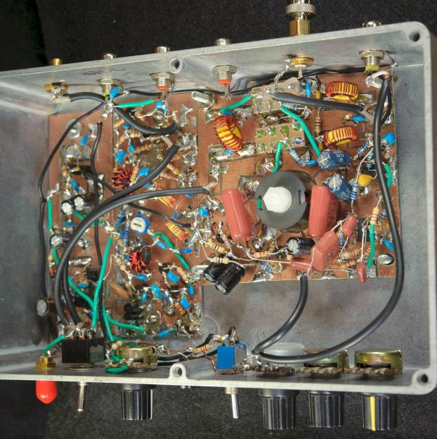
Back in the 1980s I was a budding electronics geek working in a TV repair shop. I spent most of my time lugging TVs to and from customers, but I did get a little bench time in. By then new TVs were entirely solid-state and built on single PC boards, but every once in a while we’d get an old-timer in with a classic hand-wired tube chassis. I recall turning them over, seeing all the caps and resistors soldered between terminal strips bolted to the aluminum chassis and wondering how it could all possibly work. It all looked so chaotic and unkempt compared to the sleek traces and neat machine-inserted components on a spanking new 19″ Zenith with the System 3 chassis. In a word, the old chassis was just – ugly.
Looking back, I probably shouldn’t have been so judgmental. Despite the decades of progress in PCB design and the democratization of board production thanks to KiCad, OSH Park, and the like, it turns out there’s a lot to be said for ugly methods of circuit construction.
Ugly is Beautiful
Construction methods that differ from standard surface-mount and through-hole PCB technology vary, but a decent catch-all term for these methods is “Ugly construction”. Specifics vary, but it’s one of those “You’ll know it when you see it” things. For my money, ugly style is any electronic build technique where the components are not completely mechanically anchored to a substrate, like a clad or unclad board. With through-hole and SMT, we’re used to all the terminals of each component being soldered firmly to the board, making a solid mechanical and electrical connection. Ugly eschews this approach and lets the components all hang out.

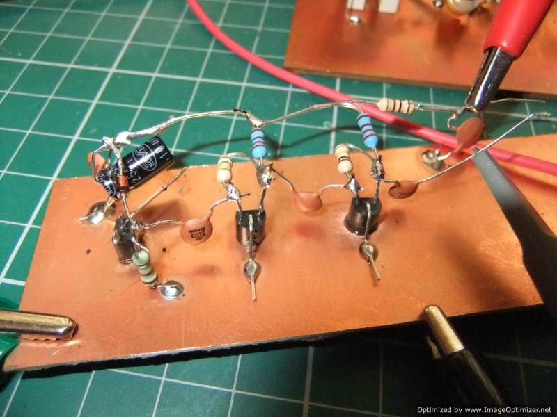
Sometimes there’s no board at all in an ugly build and the components are just soldered to terminal strips or between input and output connectors. Such builds are not terribly sound mechanically, so they’re mostly reserved for quickie prototypes. When there is a board in an ugly build, it’s generally used solely as a ground plane with only the grounded leads of components soldered down. With ground established and some semblance of mechanical stability added, the other connections are made above the board. Component leads are tied directly together or with short lengths of jumper wire, and eventually the whole circuit starts to come together. Mechanical stability can be added to a joint by running a high-value resistor to ground.
Does Ugly work? You bet! One famous example from the ham radio world is the Ugly Weekender. Designed by Roger and Wes Hayward in 1981, the Ugly Weekender is a low-power (QRP) transmitter for the 40-meter band. Started as a father and son project over Christmas break, the Weekender accomplishes a lot with just a handful of parts tacked to a plain copper-clad board. And Ugly is fast. The “Weekender” part of the UW transmitter refers to the fact that it can be built in a weekend by any reasonably skilled ham with access to a well-stocked parts bin. With no PCB to design, no tedious phototransfer or manual masking process, and no etching, the build can begin right away. I think this is the largest intangible benefit of Ugly construction – it doesn’t interrupt the creative momentum. You get an idea, you start tacking parts down, and you just follow the flow of the design.
There’s a Dead Bug in My Circuit

As you can imagine, Ugly works best for circuits that mostly use discrete components. After all, it’s got to be difficult to tack a 14-pin DIP down to a board, right? Enter the “Dead Bug” style of Ugly. As the name implies, Dead Bug builds have components with all the leads sticking up in the air like a dead bug. Sometimes the DIPs and other components are glued to the board for mechanical stability with a dab of superglue. The important point, though, is that interconnections still all occur above the board, and ground connections are short, direct and many. That huge ground plane is a key feature of Ugly, which is why it’s so often used for RF circuits.
Another benefit of Ugly is the reduction of stray capacitance. Solderless breadboards are great prototyping tools, but there’s no escaping the fact that a grid of long, parallel conductors spaced 0.1″ apart and separated by a dielectric is going to have capacitance. It’s not a lot, and it’s not a factor for every circuit, but a couple of picofarads here and there can add up to a problem. With short leads and no long parallel traces, Ugly minimizes stray capacitance and is another reason a lot of RF circuits use it.
Help for Ugly: Manhattan Style
Ugly only goes so far, though, and it’s not appropriate for every circuit. Ugly tends to be difficult to replicate – after all, when you solder four leads together in the air and support it with a 10-megohm resistor to ground, it’s a little difficult to document exactly what you did, and even a photograph doesn’t necessarily do it justice. So Ugly sometimes needs some help, and that’s where Manhattan style comes in.
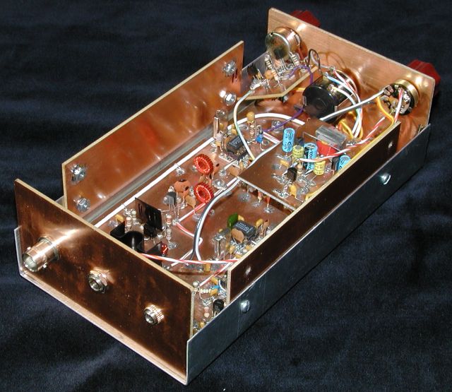
Named after its resemblance to rows of high-rise buildings, Manhattan construction uses small pads punched out of copper-clad board and glued to the ground-plane board. Insulated from the ground-plane, the small copper pads serve as junctions for terminals – no more connections hanging out in mid-air, and no more support resistors. Pads can be punched out or created with a nibbling tool, or even created directly on the backplane board. ICs can be incorporated into Manhattan builds either with tiny pads or with a larger pad with lines scored in the copper by some careful work with a saw. Dead-bugging an IC in a Manhattan build is not out of the question, either.

You might be tempted to think that Manhattan is only useful for through-hole components, but not so fast. With a little ingenuity, even surface-mount components can find their way into Manhattan builds. Following [Paul Harden]’s (NA5N) guide to Manhattan, pads and strips created of the thinner 0.031″ thick copper clad board can be glued to a thicker backplane and used to create landing pads for surface-mount parts. As with any build using SMT, things can get a bit dicey, but with enough pre-planning and the proper tools, Manhattan-SMT can result in some pretty cool builds.
Ugly and Manhattan construction are clearly not suitable for every build, but knowing these techniques can open up some doors and make it a little easier to throw a circuit together. And as [Harry Lythall] (SM0VPO) points out, “The correct construction method is any one that works. The best construction method is the one that works best.” Maybe one of these methods will work best for your next project.
Featured image: [K8IQY]’s SW30+ 30-m CW transceiver. Source.


Thanks, was an interesting read
Ugly is only skin deep. The true beauty of a project comes from within.
On my bike, I have a lighting controller which is built dead-bug style that I depend on daily for my safety when riding. In 5 or so years, this circuit has not failed me. It’s built around a LM555, diode-OR logic, and a IRF540N MOSFET.
On the other hand, I’ve had numerous commercially made tail lights fail, and one of the bikes, there’s a electronic horn constructed using veroboard that, while mostly reliable, is glitchy. I’m thinking of building one up for my other bike, using dead-bug construction.
The other place where I’ve used dead-bug construction, is in my virtual machine cluster: https://hackaday.io/project/10529/log/36511-12v-regulator-installation
Virtually all bike lights are crap, just like all flashlights. The battery is too small for a sexy sale size. Crimped and riveted straps of eroded plated steel pressure contacts! Nothing like soldered everything, including the power cells. I hope you have more steady light on that bike than intermittent lighting. The average motorist just takes “snapshots” of conditions on the fly and any flashing light not accompanied by full steady lighting is not registered as a moving vehicle. A watt or two of LED will do. Coin cells and old school AAA-AA and such can only be expensive. With a generator you will have the closest thing to free energy, power that doesn’t need a switch, Nothing to mess with
at all when you ride or park.
Well, you be the judge (no it doesn’t flash):
http://www.longlandclan.id.au/~stuartl/bikeforums/2015/03/03-commuter/img_20150303_044917_709-720×540.jpg
As someone who was trained in the US Army Air Force to be a radar technician in 1944 we snapped together circuits with alligator clips and the kind of snaps you use to close your jeans at the top of your fly. A very quick way to learn circuitry. Our final projects were soldered but the layout to perform minimum wire length was not particularly artistic. Our wiring was with colored wires to identify the various inputs and outputs.
Wow, that Manhattan style SMD is really tidy. I don’t remember having seen that before.
That nibbling tool method we covered years back is still one of my favorites. Really quick and easy since you can put it anywhere and there’s no cutting or gluing, just a quick hit with the drill to form a channel that breaks the copper pour.
I love doing point to point wiring. You can build a multitude of circuits on solder lug terminal strips. As long as leaded components remain available anyway. When I went to tech school PCB where being used in newer stuff, but all the tech school shop got where the older point to point wiring gear, so that’s what we learned to work on first. In fact building a FETVOM kit that use point o point wiring for our own private use was our soldering training bed. Because an electrician is likely to run into knob and tube wiring where where taught how to solder that properly as well. At that time while the code didn’t allow for new knob and tube installation, it allow for it’s repair. When it came to PCB they gave us box that contain the circuit board for an all American 5 AM broadcast receiver horribly busted up on purpose, we where told to get it working again. The solder skill we learned to that point, made it possible to complete the task One old timer I knew said he left the business when PCB became common place.
Don’t forget that breakout boards and strips with copper lines exist to facilitate manhattan construction. They come typically with double-sided tape on the back.
If you want to use a DIP IC, it’s fairly easy to do that neatly without buying special PCBs.
Cut a bit of Veroboard to the size of the IC, allowing an extra couple of rows above and below the IC.
Cut the tracks under the IC as usual. Take an IC socket (or you can just use the IC directly, I suppose) and bend out the leads 90 degrees. Now you can sit the IC socket on the copper side of the Veroboard on the traces and solder it, surface mount style. Now glue down the Veroboard, copper-side-up, onto your base board and you can solder on some connecting wires.
Curious, how is that better than just doing it through-hole on Veroboard like usual?
If you did that, either the IC would be under the socket and difficult to access, or the pins would be shorted together by the copper clad board beneath.
http://www.qrpme.com sells etched pads to add regular or surface-mount ICs to Manhattan projects. I have two on my workbench just now.
“For my money, ugly style is any electronic build technique where the components are not completely mechanically anchored to a substrate, like a clad or unclad board.”
“Sometimes there’s no board at all in an ugly build and the components are just soldered to terminal strips or between input and output connectors. Such builds are not terribly sound mechanically, so they’re mostly reserved for quickie prototypes.”
You mean point to point wiring and tag/stripboard wiring? Like was done since home electronics were introduced and is still done today? I’m sorry, open up an old Tektronix scope with the ceramic stripboard construction and try to convince yourself it’s ugly. At worst, point to point can be messy, but it can easily be mechanically sound enough, and does things like keeping distances between components at a minimum which is very useful in certain applications and many other benefits. Downside is it’s much slower to build and it makes troubleshooting a little harder, but just because it looks messy doesn’t mean it’s bad or inferior, and calling some vintage equipment with point to point wiring that can only be described as ‘pornographic’ as ‘ugly’ is just waving a flag from a hilltop that proclaims ‘I have bad opinions and the only good designs are the newest styles’.
Did you not understand that “ugly” is not a value judgment but rather a catch-all term for non-PCB construction?
Even if it was a value judgement, it would be one based on appearance and not functionality.
Back in the day (the late 80sish) I used to work porting Unix people’s prototype hardware (68ks and the like) we’d get all sorts of hardware in the door – one group of Swedes bought a 1st class seat to get their wire-wrapped masterpiece to Berkeley – we did notice a vague pattern though, some weird cultural thing, people from the East Coast built their proto systems up (stacking chips on each other – think Manhattan), people from the West Coast built out, sprawled (Silicon Valley still had orange groves in those days)
I don’t do any RF work anymore but here’s an idea –
One of the techniques used in the pics was to drill an isolation barrier in the existing copper surface rather than glue copper clad “dots” to the surface.
I would imaging that this would have to be done in drill press as a hand held drill would tend to spin out of control.
What if someone made a drill much like a round hole-saw for wood with a pilot bit in the middle (06. to 1.0 mm) so that it can be used with a small Dremel like drill. It could also have de-buring and a depth limit.
It could then also be used on double sided board with the center hole used to link to the other side. The width of the isolation barrier could also be chosen so that you can easily solder common SMD passives across the barrier.
Then this sort of work could be done more quickly and more creatively as you don’t need to go back and forth to a drill press.
I think there’s a HaD article covering this. Use a piece of steel tubing with a straight cut end then file a few notches for cutting teeth. In a drill press it will isolate solder pads in the copper.
https://youtu.be/ErJWhwNKnEI
I made a tool by reshaping a brad point bit to cut pads into a pcb with just a hand drill.
I have a set of three from the 1980’s. Three #68 or there abouts drills with a hole saw style hardened steel cutter that will remove the copper in a circle. Circles are .010 inch, .015 and .030. They leave a nice pad for soldering. And guess what? They are in my tool box! Now, how do you add a photo to this….
Stahler.JPG
Maybe like this…
http://i1091.photobucket.com/albums/i382/Comedicles/Latest/Share/Stahler_zps3c7bmgf0.jpg
I also really like this kind of construction, but use Kapton tape to put bigger Isolation lands on copper clad and put smaller pieces of copper tape on top of this to create the islands. While mechanical inferior (only glue holds a smd part soldered to the islands this at this stage but there are other connections soldered later on that add strength), and the bigger capacitance to ground compared to an island cutter, it sure is nice to have a process that only needs a scissor and a tweezer (apart from the copper and kapton tape) See attached picture for example, its an active hf antenna http://imgur.com/GHRMUdy (Yes, that dgmos was salvaged from a tuner can, yes it worked, yes it died presumably of esd shortly after)
If you can’t be bothered to fashion your own drill bits, spot-weld drills are available off-the-shelf for not very much and make a very nice circle cut. The ones I have have a sprung centre-pin for location, a nice touch.
Stopped by to recommend spot weld cutters, and a small round milling burr for the Dremel.
Those are not jumpers. They are “hookup wire” :-) And before vinyl insulation, at least half you time was spent stripping hookup wire or scraping varnish of magnet wire. Or the dreaded double whammy of tough wound insulation over varnished hookup wire!
My hacked together prototyping method of choice involves using a razor blade and a steady hand to selectively trim bits of copper off the FR4. Takes practice and looks terrible (especially before you clean out all the flux that collects in the grooves), but makes it possible to quickly prototype with 0.65mm-spaced TSSOPs and the like…
[examples: https://cdn.hackaday.io/images/4221791462551283770.jpg https://cdn.hackaday.io/images/5568791459970141448.jpg https://cdn.hackaday.io/images/5806781448336646148.gif https://cdn.hackaday.io/images/8653041451270571499.JPG ]
“Anything worth doing, is worth doing badly.” G.K. Chesterton
It’s important that any prototype is ugly and slightly unreliable, otherwise it mysteriously becomes the finished article made les ugly by hiding it in potting jelly.
There may be a reason this sounds like a confession.
I to started my engineering life working weekends while at school in TV repair shope and very much remember those ols valve chassis. I to remeber luging old heavey crt tvs around. Any onr tried lifting 27″ sony tv? Garate thing was with old valve tv’s was you could swap out valves realy easly.