In the last (and first) post in this series, we took a look at Eagle. Specifically, we learned how to create a custom part in Eagle. Our goal isn’t just to make our own parts in Eagle, we want to make schematics, boards, and eventually solder a few PCBs.
The board we’ll be making, like all of the boards made in this Creating A PCB In Everything series, is the Nanite Wesley, a small USB development platform based on the ATtiny85. This board has less than a dozen parts, most of which are through-hole. This is the simplest PCB I can imagine that has sufficient complexity to demonstrate how to make a board.
With that said, let’s get onto the second part of our Eagle tutorial and lay out our circuit board.
The Eagle Workflow
Although this guide to making a PCB in Eagle began with making a part, this obviously isn’t the usual workflow. Hundreds of libraries for almost every part you can imagine already exist, including the fantastic Sparkfun libraries, the Adafruit libraries, Dangerous Prototypes, and Seeed’s Open Parts Library for Eagle. In these libraries, or elsewhere on the Internet, you’ll be able to find just about every part you could possibly need.
The general overview of how to create a board in Eagle is to first create a schematic. This schematic will contain all the parts you’re going to use in your project and all the connections between these parts. After the schematic is complete, we then create the board. The board is the physical representation of a PCB, with parts, pads, and traces. This board file can be sent off to any of the usual board houses (OSHpark, Seeed, or DirtyPCBs), and in a week or two, a pile of printed circuit boards will arrive in your mailbox.
Getting Started
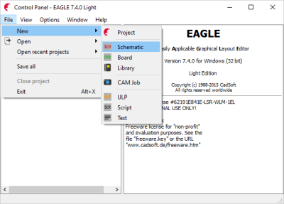
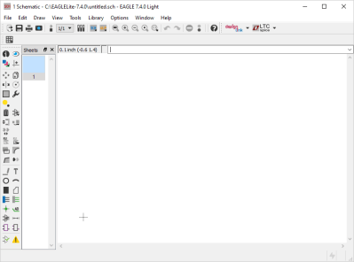
To create a schematic in Eagle, select File -> New -> Schematic in the Eagle control panel. The schematic window pops up. This is where you make your circuit. The toolbar buttons in Eagle changed since version 7, in my opinion for the worse, but here’s an overview of the buttons you’ll need to know:
 The ‘add a part’ button. This is how you browse and search through libraries for parts.
 The ‘delete’ button. Self-explanatory.
![]() The ‘move’ tool. Also self-explanatory.
The ‘move’ tool. Also self-explanatory.
![]() The ‘draw a bus’ (blue) and ‘draw an electrical connection’ (green) buttons. For this project, we will only be using the ‘electrical connection’ tool to draw connections between different components. The ‘bus’ tool does effectively the same thing, but allows you to group similar electrical connections together (as in the data or address lines between a CPU and RAM). Ignore the blue button for now.
The ‘draw a bus’ (blue) and ‘draw an electrical connection’ (green) buttons. For this project, we will only be using the ‘electrical connection’ tool to draw connections between different components. The ‘bus’ tool does effectively the same thing, but allows you to group similar electrical connections together (as in the data or address lines between a CPU and RAM). Ignore the blue button for now.
![]() The ‘name’ tool. This allows you to assign a name to individual components or electrical connections. In every board you make, you’ll want to name every connection between components.
The ‘name’ tool. This allows you to assign a name to individual components or electrical connections. In every board you make, you’ll want to name every connection between components.
![]() The ‘value’ tool. This tool allows you to assign a value to components. Your board may use the same resistor symbol over and over again, but you don’t need to make a new symbol for 22Ω and 1kΩ resistors. With the value tool, we can just assign the same part different values.
The ‘value’ tool. This tool allows you to assign a value to components. Your board may use the same resistor symbol over and over again, but you don’t need to make a new symbol for 22Ω and 1kΩ resistors. With the value tool, we can just assign the same part different values.
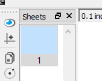 In addition to the toolbar, there’s one additional feature that bears mentioning, but isn’t really relevant to this project. The ‘sheets’ window allows you to spread your schematic over several different pages. These pages all go into the same board in the end, but it is sometimes helpful to split parts of your design up into different sheets. Put your power supply/battery management circuit on one sheet, and your microcontroller wizardry on another, for example. The free versions of Eagle only support up to two sheets, making the utility questionable. When you get to larger designs, more sheets are very helpful.
Laying Down Parts
With that out of the way, it’s finally time to start laying down parts and connecting them together. Click the ‘add a part’ button, and after Eagle thinks about it for a bit, this gigantic window will pop up:
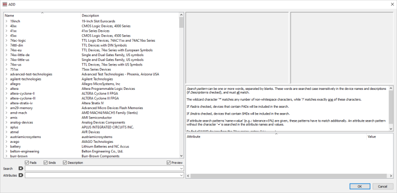
This window is how you browse and search all your libraries. Eagle comes with a few libraries already, but to really get the best bang for your buck, you’ll want to download and install the Sparkfun and Adafruit libraries in your Eagle/lib directory.
Now it’s time to start placing parts. I’d start with the microcontroller in this case, and if you’ve built your part correctly, just type “ATtiny85” into the search box and press enter. Select the part, and drop it on the schematic. For this board, we’re going to need a few more parts to complete the circuit:
- (2) four-pin through hole headers
- (2) through hole Zener diodes
- (4) through hole 1/4 Watt resistors
- (1) ceramic capacitor
- (1) 3mm LED
- (1) tact switch
- (1) micro USB port
- several symbols for ground and VCC rails.
All of these parts can be found in the Sparkfun libraries. When we find and drop all the parts on the schematic, we’ll have something like this:
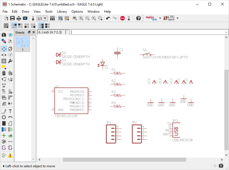
We already know what this schematic should look like; we’re merely copying the schematic we’re using for all of these Creating A PCB guides. Start by taking the symbol for the ATtiny, the capacitor, VCC, and GND and arranging them like so. Use the ‘make an electrical connection’ button to draw the lines out from the pins.

Now it’s time for the most powerful tool in Eagle. Click the Name button and assign a name to each and every one of the electrical connections on the microcontroller. Again, we’re simply copying this schematic. Name the electrical connections PB0, PB1, PB2, PB3, PB4, and NRES, just like in the schematic. Once we’re done with that, use the Label tool to give these electrical connections a label. With that done, we have a surprisingly large part of our schematic complete:
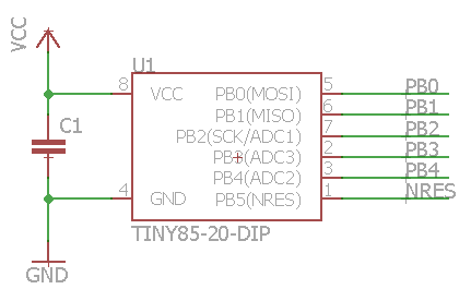
Since the rest of this schematic building exercise is simply copying the reference design while applying the techniques used previously, do that. When you’re done, you’ll have something like the schematic below. Don’t forget to use the Value tool to assign values to the capacitors, diodes, and resistors.
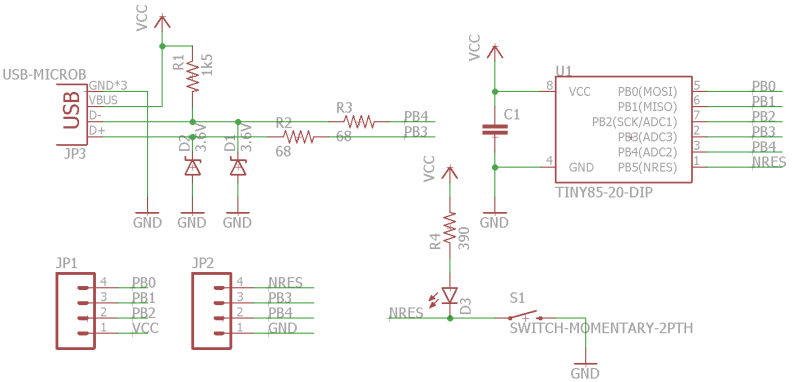
With a completed schematic, it’s time to move onto the cool part of making a PCB: laying out the board.
Designing the Board
With our schematic complete, we can create the board. To do this, simply save your schematic, and from the File menu, select, Switch to board. Eagle will ask you if you would like to create a board from the schematic. Click yes, and you’ll see something like this pop up:
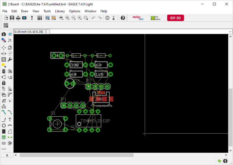
Yeah, that’s quite a mess, but it all makes sense. Let’s break down what’s going on here.
Every part in Eagle is made of two distinct representations: the package, and the symbol. The symbol is what we use to create the schematic. The package is the physical representation of the part, and what we use when creating a board. Those rectangles with green circles are the packages for every part, and the green circles are the pads — the bits of metal poking up through the soldermask that we apply solder to. You may notice the USB port is red — that’s because it’s a surface mount (SMD) part and doesn’t have holes going all the way through the PCB. The red indicates where we solder an SMD part to the top of the board. If the USB port were blue, we would solder it to the bottom of the board.
The thin yellow lines between each pad are airwires, representations of where electrical connections should go. When we start to draw traces, we’ll connect the pads together by following the airwires.
Now, with that bit of nomenclature out of the way, let’s get down to designing a board. Here are the tools we’ll need to create our board:
![]() This is the Line tool. We use this to create the outline of the board. We don’t use this to draw connections between parts – this tool is only used for laying out the outline of the board.
This is the Line tool. We use this to create the outline of the board. We don’t use this to draw connections between parts – this tool is only used for laying out the outline of the board.
![]() This is the Route tool. We use this when making electrical connections between pads.
This is the Route tool. We use this when making electrical connections between pads.
![]() This is the Ripup tool. We use this to remove traces we’ve already made.
This is the Ripup tool. We use this to remove traces we’ve already made.
 This is the Polygon tool. We use this tool when we want to fill an entire area of the board. If you want your board to be completely white, Cover the entire board with the silkscreen layer. I’m sure board houses hate this, although it does look cool.
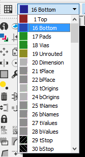 When using the Line or Route tool, we have an option of drawing only on the top copper layer of the board, on the bottom copper layer of the board, on the silkscreen layer, and even drawing negative space on a particular layer of the board. The Layer dropdown menu is how we select which layer we’re routing or drawing on.
The other tools we’ll be using are the move and delete tool. Let’s begin by first drawing the outline of the board in the Milling layer. Use the Line tool and draw a rectangle on the Milling layer. Then start placing the parts like in the reference board. You’ll get something like this when you’re done:
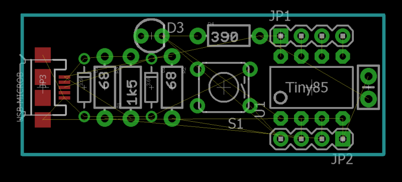
Drawing signals
For the time being, we’re going to ignore VCC and GND. We’re only going to concern ourselves with routing the signals between the parts that aren’t power or ground. Click the Route tool, and we can start laying down traces. We’ll want to start laying down traces on the Top layer of copper, or in Eagle nomenclature, the red layer.
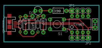
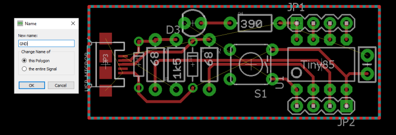
To the right is our first attempt at routing the board. It’s pretty good, but there are still a few airwires hanging around that need to be connected, but that’s going to be a little hard to route. Instead of routing each pin individually, let’s draw a Polygon and do what’s called a copper pour. This is an area of copper electrically connected to a signal, VCC, or GND. In this case, we’re going to do a copper pour on the top layer of the board and connect it to GND. That’s a good idea in this case because the large pads on the USB connector are electrically connected to GND. To do this, just click on the Polygon button, and draw the pour using the board outline as a guide. Name this polygon GND, and click OK. Nothing happens.

All of those GND pins are connected together with a copper pour, but Eagle isn’t showing it. We need to force Eagle to show these changes, and we do that with a button on the toolbar. This button is labeled ‘Calculate shortest airwires’, and the icon makes little sense.
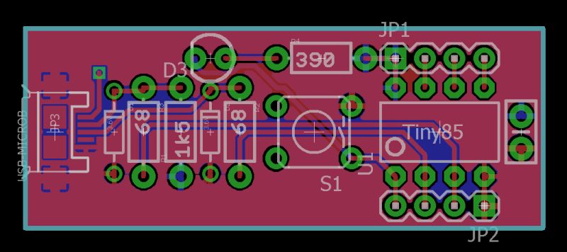
With that done, we can create another copper pour on the bottom copper layer, named VCC. From there, all we need to do is draw one or two traces on the bottom copper layer to connect the rest of the pads together, and we have this, a completed board, ready to be sent off to OSHpark, Seeed Studio, or DirtyPCBs.
Vias
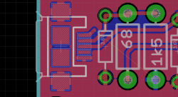
If you’re exceptionally clever or are just following along, building this board as you’re reading it, you’ll notice a severe oversight:
One pin on the USB port isn’t connected to anything — there’s a tiny little airwire connecting that pin to the closest pad connected to VCC, telling you this is something you need to route. The naive way of doing this is routing a trace around all your components, but that’s dumb and we’ll get to that in the Fritzing tutorial. The much easier way of connecting this pin to VCC is simply drilling a hole through the board.
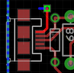
This is a via. It’s a hole, or pad, drilled right through the board. The inside of this hole is either electroplated or lined with a copper ferrule (very weird and very rare), and connected to traces on the top, bottom, or inner layers of a board. If you want to send a trace to another layer of the board, you need a via.
To put a via on your board, simply draw a trace to somewhere out of the way, and click the middle button on your mouse. This will change the layer you’re drawing traces on. Draw a little bit on the second layer, and let go. A trace will automagically appear.
The Board’s Done. Save everything, and we’re done creating a board. There’s still more to do, in the next (and final) installment of the Eagle portion of this Creating A PCB series, we’re going to send this board off to a fab. This means Design Rule Checks (DRC), creating Gerbers, checking the Gerbers, and a quick bit on my favorite part of Eagle, putting custom art on a board.
As always, if you have any feedback for this post, or the Creating A PCB series in general, leave it in the comments.




What’s the purpose of this publication in Hackaday ? If someone is looking for a Eagle tutorial (or any others PCB software) there is already many tutorials very easy to find on the internet.
It’s for content. And for people like me, that like the authors on this website.
What’s the point in making any product if there is already a similar product on the market?
maybe there’s a hack somewhere in the tutorial?
it’s interesting to some of us. And… you haven’t made a hack/project yet so they can write an article about it :-) instead of making a tutorial.
It’s not just this tutorial, it’s the fact that we’re going to see _the same board_ made in several different EDA packages. Plus HaD has a pretty big user base, so we’ll hopefully get some good comments and suggestions from users.
I’d like to see more kicad articles. There are certainly a few.
But damn is it getting powerful. Like.. really.
Sure not all the gizmos and doodads of Altium, but can make boards just as good as if you have the skills to work it like a boss.
Yeah it’s got quirks. And some things demand really painful work around. But those will iron out eventually.
Hope you’ll include both chemical and CNC final realization of the product for DIY.
Usually I prefer to draw the ground plane when most of the wires have already been routed, typically when I reach 10 or less unrouted wires. For DIY fabrication I keep the isolation at 24 mils to reduce the chance of a short circuit during the hand soldering process.
On my previous remark on this series of articles I’ve endorsed the use of single sided boards for ince they are far easier to replicate at home using techniques like toner transfer. Since talk is cheap I’ll show you the board, lol!!
https://cdn.hackaday.io/images/6723661474669078258.png
It’s a commendable attempt to make a single-sided board, but yours could be much improved by a change of technique. Many Eagle users seem to rely on having the ground connection provided by a copper fill that’s added to the board after everything else is routed. While this is certainly convenient, it makes for generally bad ground connection, which can lead to all kinds of problems down the road.
For example, look at the very poor placement of C1. C1 should be directly connected to Vcc and GND, as close as possible to the Microcontroller’s power input. Trace length should be kept to a minimum. The Vcc connection is just about okay, could be better, could be worse, but it’s okay. The GND connection is horrible, GND from the capacitor snakes along almost the whole board before it meets GND of the microcontroller.
Agree with you. One shall not rely solely on the ground paths provided provided by the ground planes. I noticed the connection of the capacitor, but I considered it acceptable for the purpose of this project. If you decompose the ground plane you will se that all connections converge to the same place under the diodes. See that the ‘negative’ lead of the capacitor meets the ground pin of the microcontroller at the same point, as the anodes of the zeners. It might be better, it can always be better but then again it’s good enough and far far better than the average proto-board builds.
Also, I’ve followed other constraints that might not be visible at a first sight, like leaving the right side of the board free of any component just in case you need to use a screwdriver to remove the IC; and use the least board area as possible (no wasted spaces).
And thanks for sharing your tips.
While it is not ideal, could at least use S1 to bridge the ground connection. The Top right hand corner of S1 is internally connected to bottom right.
The placement and routing could be improved by having U1 in the middle and S1, LED1 and C1 on the right edge.
Yeah, that’s a good tip, thanks! But I left S1 as it is just to stick to the original project. A track between pins 1 and 2 would be another solution, but as I’ve answered to f_ it is good enough. The same for the right side of the board. I left it free of components because it gets easier to take out the microcontroller with a screwdriver when the ATTiny needs to be replaced or taken out to be reprogrammed which happens seldomly in the Tinies with bootloader (not a fault of the project, tough).
You could rotate U1 90 degrees so that you can pry it out but still have the chip in the middle. I usually try a few different routing and placements for the best signal/power integrity.
I usually leave switches, LED on the edge. For I/O connectors, either they are on opposite sides if needed or just on one edge. 90 degrees or whatever each way takes up lots of real estate by the time you plug in all the cables. and look sloppy.
Nice! Haven’t thoght about rotating the chip by 90 degrees! Surely it is a better design specially because of the button at the edge of the board! I’ll give it a try, and this time I’ll use the switch as a jumper, if necessary.
Done! Both in Eagle and in Kicad!
https://cdn.hackaday.io/images/2587231474906828751.png
https://cdn.hackaday.io/images/1821474906934498.jpg
Saw you new layout. If you rotate the other 90 degrees (anticlockwise), you’ll get the USB signals on the lefty side and button on the right side. USB Data line are twisted, but they could be swapped at the USB connector side.
Yet I’ve been wondering that although the chip at 90 degrees make the eventual replacement easier, it turns the connection of jumper wires somewhat messy since they’ll be laid over the components, don’t you think?
It is very interesting what comes when considering the real life usage of any project…
fwiw, i lay down my power planes first thing, as it eliminates a bunch of air wires, and it lets me keep an eye on whether or not i’ve split one in two.
I think its a personal preference, then. But I have some other reasons why I left the ground planes to the end. The ground planes kinda blind me from the open spaces that I have to route the wires, and they interfere in the counting of unrouted wires because often you do a track that interrupts the path of the ground wire and the net count of unrouted wires remains the same. Nevertheless I usually do some of the ground connections with ordinary wires during the routing, then at the end I pour the ground planes.
Anyway, thanks for sharing your tips.
I know you don’t care, but other people might: You’re doing it totally wrong. Power and Ground are the most important connections, which is why they are layouted FIRST. You certainly don’t slap an indiscriminate copper pour on your board to provide power and ground; this will lead to all sorts of problems when making serious designs.
Could you please provide an example or expand on what you’ve said? I’m quite interested.
Power I would route with a thick track or use an island if it help with minimizing the parasitic of decoupling caps.
I tend to use ground fills on both sides and try to stitch them together with vias to make sure that return path for the signals are not interrupted. PCB vendors no longer charge for vias these days.
Return path is the power/ground plane under a signal track. If there is a break, the return current will be force to go around – increasing its loop areas or for a slot antenna (if the break is large). Bad for EMC and signal quality.
It doesn’t matter if you route it first or last, As long as you make sure the supply tracks are thick enough to carry the current (easily). I prefer to route the signals first and later snake the positive power supply track through the pcb. I generally use 12 mil for signals and 16 or 24 mill for supply. For ground I also use a big pour on both sides with via’s
What would be best for me?
I am currently prototyping with all surface mount on single sided boards made in-house.
There is always programmable logic and I use that to rout which makes things easier for single sided. Because the routing is done in programmable logic, I don’t bother with a schematic.
I start with the PCB layout and just make footprints as needed. I use express PCB because it is so simple and fits the unusual workflow but it annoys me that I can’t place QFP’s at a 45 degrees angle and I want to move to double sided.
Any recommendations?
In Eagle you can put the cursor at the “Angle” drop down box (where is written 0, 90,180,270) and write the angle you want (45 for instance).
Another way is using the “i” icon (properties) and change the value of the angle to the value you want.
simple like that!
A schematic is also part of the documentation of what you are connecting with a level of abstraction. This is why frizing wiring diagrams are garbage for uinderstanding.
In the open source world if someone want to build your project using a different CAD system and/or different packages of chips, they can at least transcribe it.
One of the benefits with CPLD / FPGA is that I can build the hardware first and then decide on the schematic design and program it in. I can then do the schematic last once it has been designed, programmed, debugged, re-programmed and tested.
When you get to the article about sending it off to a PCB manufacturer, don’t forget the Eagle plug-in that helps you get PCB manufacturing prices (http://hackaday.com/2016/09/11/this-eagle-script-gets-quotes-for-your-boards).
Mandatory pre-design step for anyone who will have their boards made by a fab: figure out which are the restrictions for the cheapest boards. If you can deal with those restrictions, design your board around them.
Example: dirty PCBs only does small orders for 5×5 or 10x10cm sizes, and they won’t do single sided. You might want to pick a suitable standard size to accommodate your project instead of an arbitrary size, and to accomplish that you might want to put a few components on both sides of the double sided board (they don’t do single sided). A homemade board’s constraints are opposite: you can get any size of board easily, but doing double sided is a PITA. So, remember to set your designer mind to the proper fab constraints.
They can do up to 60x60cm. And for that price you get an extra layer extra ;)
Mandatory pre-design step for anyone who will have their boards made by a fab: figure out which are the restrictions for the cheapest boards. If you can deal with those restrictions, design your board around them.
Example: dirty PCBs only does small orders for 5×5 or 10x10cm sizes, and they won’t do single sided. You might want to pick a suitable standard size to accommodate your project instead of an arbitrary size, and to accomplish that you might want to put a few components on both sides of the double sided board (they don’t do single sided). A homemade board’s constraints are opposite: you can get any size of board easily, but doing double sided is a PITA. So, remember to set your designer mind to the proper fab constraints.