How To Do PCB Art In Eagle

Last month I had the pleasure of creating a new piece of hardware for Tindie. [Jasmine], the queen bee of Tindie, and I designed, developed, and kitted three hundred Tindie badges in ten days leading up to DEF CON. The badges were a complete success, they introduced soldering to a lot of people, and were loved by all.

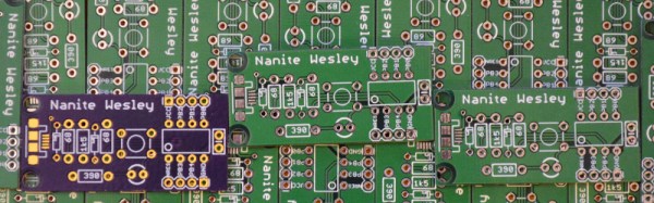
This badge was such a rousing success, it’s now official Tindie swag. We’ll be handing out a few of these blinky badges at upcoming events. But as of right now we’ve already handed out our entire stock, that means we need to build more. The second run meant ordering a thousand PCBs.

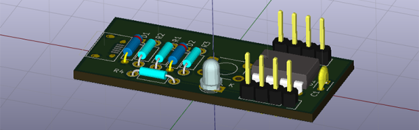
We could just do another run, and order a few more PCBs from the Gerbers I’ve already designed. I’m not really happy with the first version of this badge, though, and this is an opportunity to improve my design. This also gives me an opportunity to demonstrate my workflow for creating artistic boards in Eagle.

Effectively, what I’ll be demonstrating here is the creation of the Benchoff Nickel. A few months ago, [Andrew Sowa] took a portrait of yours truly, changed the colors to what is available on a normal OSHPark PCB, and turned that into different layers in KiCad. There are a few differences here. Firstly, I’ll be using a blue solder mask, although the same technique can be applied to green, red, yellow, white, or black soldermask. Secondly, this is Eagle, and I’m going to do the majority of the work with a BMP import. This is the fast and easy way to do things; if you want a KiCad tutorial, check out [Andrew]’s work, or my overly-involved multiple silkscreen process for KiCad. I don’t recommend this overly-involved process if you can help it. It took 20 hours to do the art for my previous project in KiCad, and I estimate it would have taken two in Eagle.

With that said, here’s the easy, cheap, and fast way of doing artistic boards in Eagle.

Continue reading “How To Do PCB Art In Eagle”

Panelizing Boards The Easy Way

For reasons that will remain undisclosed until some time in the future, I recently had a need to panelize a few PCBs. Panelization is the art of taking PCB designs you already have, whether they’re KiCad board files, Eagle board files, or just Gerbers, and turning them into a single collection of PCBs that can be sent off to a fab house.

Now this is panel racing

If you’re still wondering what this means, take a look at the last board you got from OSH Park, Seeed, Itead, or Dirty PCBs. Around the perimeter of your board, you’ll find some rough spots. These are ‘mouse bites’ and tabs, places where the boards are strung together to form a gigantic rectangular panel sent off to a manufacturer. You can check out this great interview with [Laen] from OSH Park to get an idea of how this works, but the basic process is to take a bunch of Gerbers, add tabs and mouse bites, solve the knapsack problem, and send the completed panel off to a board house.

Panelizing boards is something most of us won’t have to do often. Really, you only want a panel of boards when you’re manufacturing something. For small-scale production and prototypes, bare boards will do just fine. Simply by virtue of the fact that panelizing boards is far less common than throwing some Gerbers at OSH Park or Seeed, there aren’t many (good) tutorials, and even fewer (good) tools to do so. This is how you panelize boards quickly and easily using Open Source tools.

Continue reading “Panelizing Boards The Easy Way”

Creating A PCB In Everything: Upverter

For the last five months, I’ve been writing a series of posts describing how to build a PCB in every piece of software out there. Every post in this series takes a reference schematic and board, and recreates all the elements in a completely new PCB tool.

There are three reasons why this sort of review is valuable. First, each post in this series is effectively a review of a particular tool. Already we’ve done Fritzing (thumbs down), KiCad (thumbs up), Eagle (thumbs up), and Protel Autotrax (interesting from a historical perspective). Secondly, each post in this series is a quick getting started guide for each PCB tool. Since the reference schematic and board are sufficiently complex for 90% of common PCB design tasks, each of these posts is a quick how-to guide for a specific tool. Thirdly, this series of posts serves as a basis of comparison between different tools. For example, you can do anything you want in KiCad and most of what you want in Eagle. Fritzing is terrible, and Autotrax is the digital version of the rub-on traces you bought at Radio Shack in 1987.

With that introduction out of the way, let’s get cranking on Upverter.

A little bit about Upverter

Upverter was founded in 2010 as an entirely web-based EDA tool aimed at students, hobbyists, and Open Hardware circuit designers. This was one of the first completely web-based circuit design tools and Upverter’s relative success has been a bellwether for other completely web-based EDA tools such as circuits.io and EasyEDA.

I would like to take a second to mention Upverter is a Y Combinator company (W11), which virtually guarantees this post will make it to the top of Hacker News. Go fight for imaginary Internet points amongst yourselves.

Upverter is a business after all, so how are they making money? Most EDA suites offer a free, limited version for personal, hobbyist, and ‘maker’ projects, and Upverter is no exception. The professional tier offers a few more features including CAM export, 3D preview, an API, simulation (coming soon), BOM management, and unlimited private projects for $125 per seat per month, or $1200 per seat per year.

To give you a basis of comparison for that subscription fee, Eagle CAD’s new license scheme gives you everything – 999 schematic sheets, 16 layers, and unlimited board area – for $65 per month, or $500 per year. Altium’s CircuitStudio comes in at $1000 for a one-year license. There are more expensive EDA suites such as Altium Designer and OrCAD, but you have to call a sales guy just to get a price.

Upverter is positioning itself as a professional tool at a professional price. There are better tools out there, of course, but there are thousands of businesses out there designing products with tools that cost $500 to $1000 per seat per year. In any event, this is all academic; the Hackaday crowd gravitates towards the free end of the market, whether that means beer or speech.

A big draw for Upverter is their Parts Concierge service. You’ll never have to create a part from scratch again, so the sales copy says. Apparently, Upverter is using a combination of very slick scripts to pull part layouts off a datasheet and human intervention / sanity check to create these parts. Does it work? We’re going to find out in the review below.

Continue reading “Creating A PCB In Everything: Upverter”

Creating A PCB In Everything: Creating A Custom Part In Fritzing

This is the continuation of a series of posts where I create a schematic and PCB in various EDA tools. Already, we’ve looked at Eagle CAD, KiCad, and took a walk down memory lane with one of the first PCB design tools for the IBM PC with Protel Autotrax. One of the more controversial of these tutorials was my post on Fritzing. Fritzing is a terrible tool that you should not use, but before I get to that, I need to back up and explain what this series of posts is all about.

The introduction to this series of posts laid it out pretty bare. For each post in this series, I will take a reference schematic for a small, USB-enabled ATtiny85 development board. I recreate the schematic, recreate the board, and build a new symbol and footprint in each piece of software. That last part — making a new symbol and footprint — is a point of contention for Fritzing users. You cannot create a completely new part in Fritzing. That’s a quote straight from the devs. For a PCB design tool, it’s a baffling decision, and I don’t know if I can call Fritzing a PCB design tool now.

Continue reading “Creating A PCB In Everything: Creating A Custom Part In Fritzing”

Creating A PCB In Everything: KiCad, Part 3

This is the third and final installment of a series of posts on how to create a PCB in KiCad, and part of an overarching series where I make the same schematic and board in dozens of different software tools. A few weeks ago, we took a look at making a schematic in KiCad, and more recently turned that schematic into a board ready for fabrication.

For our KiCad tutorials, we’ve already done the basics. We know how to create a PCB, make a part from scratch, and turn that into a board. This is the bare minimum to be considered competent with KiCad, but there’s so much more this amazing tool has to offer.

In part three of this KiCad tutorial, we’re going to take a look at turning our board into Gerbers. This will allow us to send the board off to any fab house. We’re going to take a look at DRC, so we can make sure the board will work once we receive it from the fab. We’re also going to take a look at some of the cooler features KiCad has to offer, including push and shove routing (as best as we can with our very minimalist board) and 3D rendering.

Continue reading “Creating A PCB In Everything: KiCad, Part 3”

Creating A PCB In Everything: KiCad, Part 2

This is the continuation of a series where I create a PCB in every software suite imaginable. Last week, I took a look at KiCad, made the schematic representation for a component, and made a schematic for the standard reference PCB I’ve been using for these tutorials. Now it’s time to take that schematic, assign footprints to parts, and design a circuit board.

Continue reading “Creating A PCB In Everything: KiCad, Part 2”

Creating A PCB In Everything: KiCad, Part 1

This is the continuation of a series of articles demonstrating how to Create A PCB In Everything. In this series, we take a standard reference circuit and PCB layout — a simple ATtiny85 board — and build it with different PCB design tools. Already, we’ve taken a look at the pre-history of PCB design with Protel Autotrax, we learned Fritzing is a joke for PCB design, and we’ve done a deep dive into Eagle. Each of these tutorials serves two purposes. First, it is a very quick introduction to each PCB design tool. Second, this series provides an overall comparison between different PCB design tools.

Now, finally, and after many complaints, it’s time for the tutorial everyone has been waiting for. It’s time for KiCad.

No, like the head of the Bajoran clergy

Although KiCad (pronounced ‘Kai-Cad’ like the head of the Bajoran clergy, not ‘Key-Cad’ like the thing that goes in a lock) is the new hotness when it comes to PCB design. The amazing growth of KiCad installations over the past few years is a long time coming. In development since 1992, KiCad has cemented itself as the premier Open Source PCB design suite, and since 2013 CERN has been making contributions to the project. More recently, the KiCad project has been showing off some amazing new features. These include 3D rendering of boards, interactive routing, push-and-shove, simulation, and dozens of other features that put it on a path to being on par with the top of the line EDA suites. Add in some great community contributions, and you have something really, really amazing. All of this is wrapped up in an Open Source license, free as in speech and beer. If you’re looking for the future of PCB design, Eagle is going to get very good but KiCad is almost there now while being Open Source.

Continue reading “Creating A PCB In Everything: KiCad, Part 1”