This is the third and final installment of a series of posts on how to create a PCB in KiCad, and part of an overarching series where I make the same schematic and board in dozens of different software tools. A few weeks ago, we took a look at making a schematic in KiCad, and more recently turned that schematic into a board ready for fabrication.
For our KiCad tutorials, we’ve already done the basics. We know how to create a PCB, make a part from scratch, and turn that into a board. This is the bare minimum to be considered competent with KiCad, but there’s so much more this amazing tool has to offer.
In part three of this KiCad tutorial, we’re going to take a look at turning our board into Gerbers. This will allow us to send the board off to any fab house. We’re going to take a look at DRC, so we can make sure the board will work once we receive it from the fab. We’re also going to take a look at some of the cooler features KiCad has to offer, including push and shove routing (as best as we can with our very minimalist board) and 3D rendering.
DRC
DRC, or Design Rule Check, is an automated process where the software checks the design of a board file. If traces are too close together, DRC will flag that. If holes are too small, DRC will notice that, too. If nets should be connected but aren’t, DRC is going to find that and tell you. The last time we took a look at DRC was with Eagle. Yes, Eagle has DRC, and here are two magnificent examples of it:


 On the left, you see one of the problems with a specific Eagle library. Notice how all the pads for that component are touching? No, that won’t work, and no, Eagle didn’t catch that. On the right, you see what happens when you don’t run DRC in Eagle.
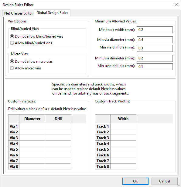
KiCad is more forgiving than Eagle. You simply can’t connect traces on different nets. KiCad will not allow you to move a trace onto a pad it shouldn’t be connected to like [Quinn]’s above example. That doesn’t mean you can get away with anything when designing a PCB; fab houses still have design rules, like a minimum track width of 6mil, minimum drill diameters, and support for blind, buried, and micro vias.
Before you start laying out your PCB, it’s a good idea to check out the design rules for a board house before placing parts and drawing traces. The design rules for Seeed Studio can be considered the least common denominator — if you can make a design with these rules, you can have your board manufactured everywhere. Practically, this means a minimum trace width of 10mil, a minimum separation of 10mil, and a minimum hole size of 0.3mm.
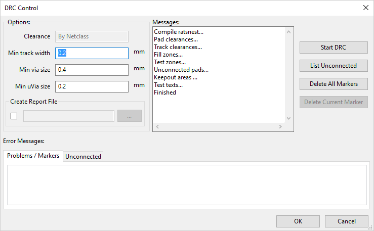
Once the design rules are set, build your board and run a DRC before generating your Gerbers from the Tools -> DRC menu. Any problems will automagically show up.
Exporting Gerbers
For the last few months, OSHPark has accepted native KiCad uploads. If you want to send your board off to OSHPark, all you need to do is drop your board file right onto their upload interface. What happens if you’re sending your board off to Seeed Studio, DirtyPCB, or any other board house? There, you’re going to have trouble. You’ll need to generate Gerber files for these board houses.
Gerbers are vector files for 2D images, and each individual file represents one layer of the board. A single Gerber file tells the board house exactly how to build the top copper layer, while another tells the board house where to put the bottom silkscreen and so on. The standard names (more precisely, the file extention) for each of these layers are:
- Top Layer filename.GTL
- Top Solder Mask filename.GTS
- Top Silkscreen filename.GTO
- Bottom Layer filename.GBL
- Bottom Solder Mask filename.GBS
- Bottom Silk Screen filename.GBO
- Board Outline filename.GKO
- Drills filename.TXT
That’s all well and good, but how do you create these files? From PCBnew, go to File -> Plot, and check out the window that pops up.
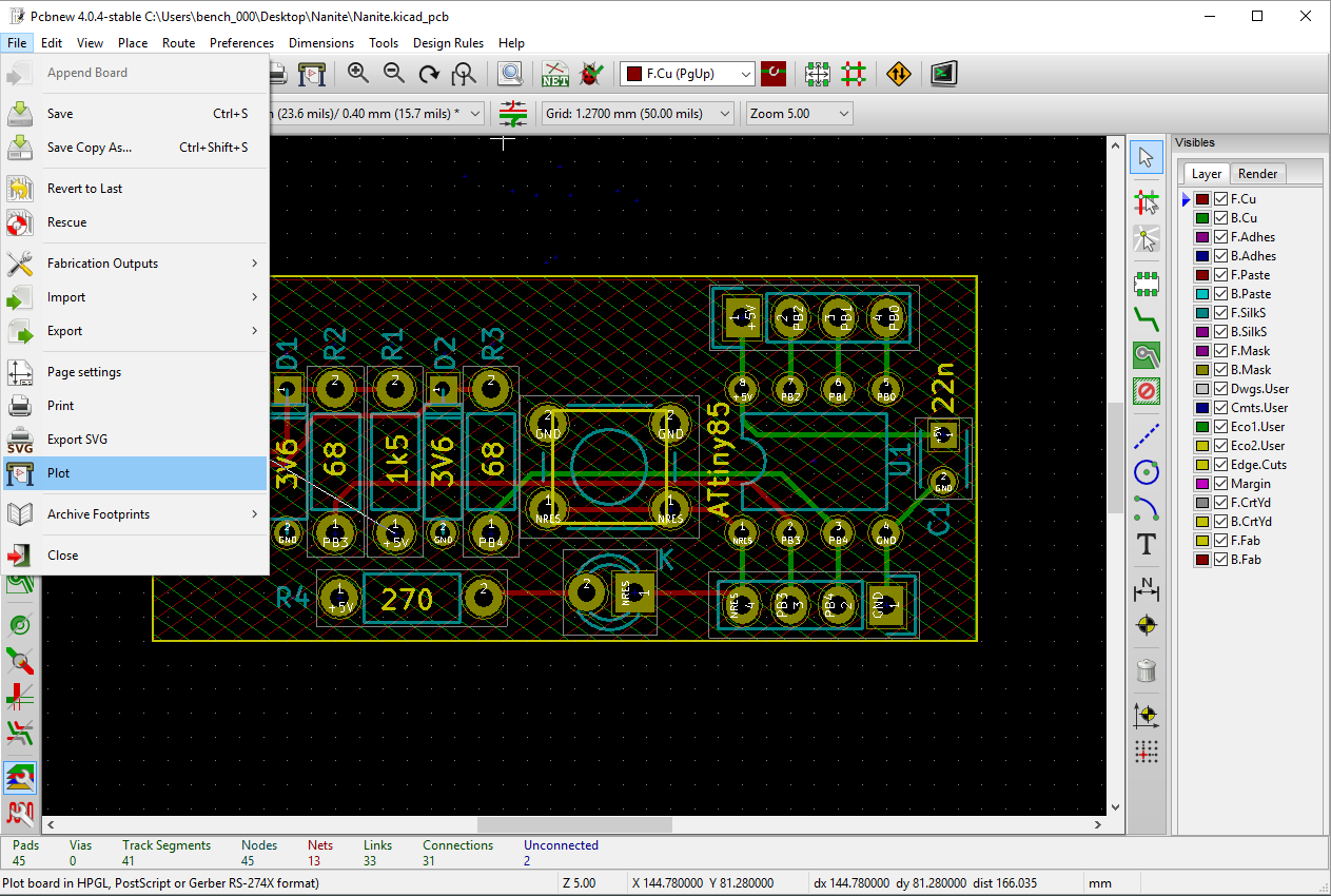
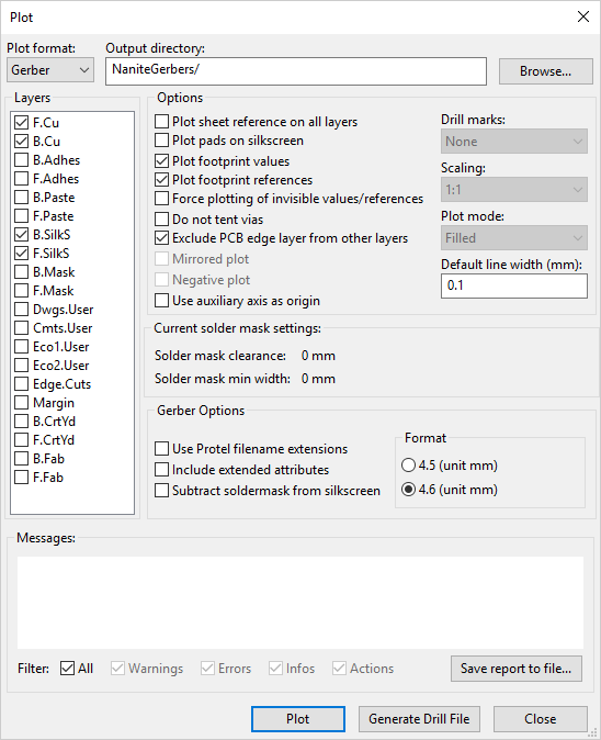
The plot window gives you a few options. To generate your Gerbers, select the following layers for a two-layer board:
- F.Cu and B.Cu – these are your front and back copper layers, and will have the file extension .GTL and .GBL.
- F.SilkS and B.SilkS – this is the front and back silk screen, with file extensions .GTO and .GBO.
- F.Mask and B.Mask – this is the front and back soldermask. What is the difference between a silk screen and soldermask? Go look at a Raspberry Pi or an Arduino. The silk screen is white, the solder mask is green or blue. The silk screen is (mostly) for outlines of footprints and names of components. The soldermask protects the copper layer from corrosion and (surprise) keeps solder off the traces. The file extentions are .GTS and .GBS.
- Edge.Cuts – this is the board outline, with the file extension .GKO.
![]() Select all of these layers, then take a look at the options you have. If you want to plot the values and references for each part on the silk screen layer, select ‘Plot footprint values’ and ‘Plot footprint references’. To save one email between you and your fab house, select ‘Use Protel filename extensions’ under the Gerber Options box. Select the output directory for your Gerbers and hit ‘Plot’.
Select all of these layers, then take a look at the options you have. If you want to plot the values and references for each part on the silk screen layer, select ‘Plot footprint values’ and ‘Plot footprint references’. To save one email between you and your fab house, select ‘Use Protel filename extensions’ under the Gerber Options box. Select the output directory for your Gerbers and hit ‘Plot’.
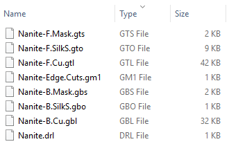 That’s not quite all there is to do, because you still need the drill file. The Drill file is the black sheep of the Gerber format. I’m not even sure it is part of the Gerber format, but like language, reality is defined by common parlance so we’ll just say the drill file is also a Gerber.
The Drill file is simply a gigantic file telling a CNC router where all the holes for the vias need to go. Press the ‘Generate Drill File’ button, don’t worry about the options, and save a drill file with the rest of your Gerbers.
To the right is what you’ll end up with: a bunch of files with weird file extensions. Put all of these files in a ZIP archive, and drop them onto the upload page for OSHPark, DirtyPCB, or Seeed Studio. Even Advanced Circuits will take Gerbers.
Additionally, there are a few more interesting options to select when generating Gerbers. The ‘Subtract soldermask from silkscreen’ gives more definition to the silkscreen itself, and if you’re ever going to experiment with the artistic side of PCB manufacturing, you would do well to hit that option for one of your board revisions.
Also, KiCad has built-in support for tented and untented vias. What are tented vias? Check this out:


The standard Arduino Leonardo is actually a very pretty board with visible traces snaking around under the soldermask. The vias for these traces are covered with soldermask. This is called a tented via. The reason for doing this is to prevent an accidental short with the via’s annular ring. The value of tented vias is obvious on an Arduino board — kids are going to stick pins in vias and generally make a mess of things. Untented vias, on the other hand, don’t have soldermask over the annular ring. This is good for reworking boards, but the finished product isn’t as pretty.
Yes, you can do tented or untented vias in other PCB design programs. I’ve done them in Eagle, but the process there is a little backwards and doesn’t make a whole lot of sense. A single button to tent (or untent) vias in KiCad is a really neat feature.
Interactive Router And 3D
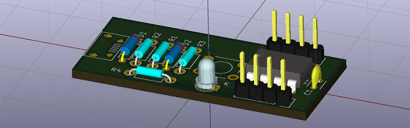
KiCad has a lot of features that are well outside the usual workflow that goes into ‘creating a PCB’, but some of these tools are really, really cool. From the Pcbnew window, select View -> 3D Viewer, and you’ll get something that looks like this:
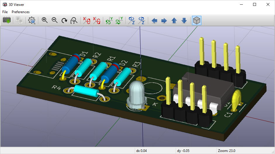
 That’s a 3D model of the board we’ve been making, with most of the parts automatically placed in their respective positions. With this model, you can export to VRML, import into OpenSCAD, and turn your electronic design into a mechanical design. The intersection of PCB and mechanical design is sort of a holy grail for engineers, and very few tools have the ability to model electronic components in physical space like KiCad. Altium can do it (and can do it well), and Eagle will be getting this ability soon (because Autodesk). If you ever need to make an enclosure for one of your PCBs, this is how you do it.
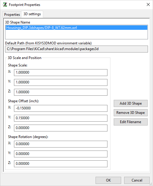
There is one trick I would like to mention regarding the 3D view. Some parts won’t have 3D models when you first open up the 3D view. That’s easily fixed – just click on the part in Pcbnew and use the hotkey ‘E’. This opens up the Footprint Properties window, with a tab for 3D settings. Here, you can select a 3D shape from the standard KiCad VRML files, and scale and offset these shapes to fit your board.
Lastly, let’s take a look at KiCad’s interactive router. This is an extremely powerful feature of KiCad that makes laying out huge boards a lot easier. By selecting a single trace and moving it around the board, the interactive router will move other traces out of the way. It will also route a trace from point A to point B using the most efficient path, without intersecting other traces. The best example of this comes from one of the KiCad devs:
I would demonstrate this on my tiny, simple board but there simply aren’t that many traces for the interactive router to be interesting.
That’s it for KiCad
In part one of this KiCad tutorial, I went over how to create a schematic. Part two covered how to make a part from scratch and turn that schematic into a PCB that’s ready to head off to fabrication. Now, after six thousand words you know how to make a schematic, a footprint, a package, a PCB, and make sure everything is correct.
We’re done with KiCad, fulfilling the constant requests I’ve gotten since starting this series of posts. Now, finally, I can turn my efforts to Open Source PCB design tools you shouldn’t use. In the next post of this series, I’m going to be covering something unprecedented. I will have a tutorial on how to create a part in Fritzing from scratch. This has never been documented before, and even the Fritzing devs say it’s impossible. If you’re wondering, yes, the bounty I placed on a tutorial for creating a part from scratch has been claimed. Until then, keep not using Fritzing because it’s still terrible. Use KiCad.


RE: Generating gerbers – KiCad generates mill outline layer with the .GM1 extension, which is not recognised by some board houses. Simply rename it and you’ll be fine.
For Hackaday.io inhabitants – we have the KiCad Central, come to share your tips&tricks and get answers to your questions! https://hackaday.io/project/7431
that’s why you click the protel extension checkbox and everything is smooth sailing from there on out.
Just checked it, I have those enabled and I still get GM1. KiCad 4.0.4 (stable)
I could see that 3D model coming in handy in the educational market.
as a professional hardware designer, the 3D model is essential, electronics typical come in cases or housing, the 3D model makes the design of that component significantly easier.
very nice writeup! is kicad finally growing on ya, brian? ;-)
There are limitations. My next *big* project is going to be an artistic-ish board, and for that Eagle is still the best. Other than that, yeah, go learn KiCad.
Disagree. Just do it all in an SVG editor. For the rest, I can show you how to get it into KiCad (still think it’s comparable to EAGLE in that respect).
Source: 2015 Hackaday Supercon badge
DO IT IN KICAD YOU LAZY BUM
Check out https://github.com/mtl/svg2mod if you do want to consider doing it with Inkscape and KiCAD.
I’m currently using Eagle to design a fairly big (think BeagleBone cape sized) and very busy board crammed with components. That means layout and routing are a huge pain, and KiCad’s push & shove feature is making me very envious right now.
I’d switch in a heartbeat if not for the big Eagle library of parts I’ve built up over the years.
Isn’t it possible to import eagle libbraries into Kicad?Though i read about something like that a while ago
I don’t understand why people still use Eagle lol
very cool. thanks for providing such accessible and complete tutorials. also very nice that you’re showing multiple methods and being systematic. much appreciated.
Yeah, this is a great series of articles. I’m looking forward to this Fritzing one though. The suffering should be palpable.
The end summary seems to be lacking Kicad part 2.
I’m wondering if Brian will put gschem pcb workflow to don’t use category.
Just a heads up that you can enable realistic render when in 3D mode, it looks way better then.
Downloading now, but I remember when one used “puppets” and plastic sheets laying everything out by hand and taping between them. We’ve come very far.
Epic tute, thanks Brian.