For the next post in the Creating A PCB series, we’re going to continue our explorations of Eagle. In Part 1, I went over how to create a part from scratch in Eagle. In Part 2, we used this part to create the small example board from the Introduction.
This time around I’ll be going over Design Rule Check (DRC) — or making sure your board house can actually fabricate what you’ve designed. I’ll also be covering the creation of Gerber files (so you can get the PCB fabbed anywhere you want), and putting real art into the silkscreen and soldermask layers of your boards.
The idea behind this series is to explore different EDA suites and PCB design tools by designing the same circuit in each. You can check out the rest of the posts in this series right here.
DRC – Design Rule Check

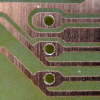
Board houses can’t produce PCBs with infinite resolution. There are limits to their process and when designing a PCB you can’t put traces too close together. The limits for each board house should be available somewhere on their web page, but generally you’re looking at a minimum trace width of 6 to 8 mil, a minimum trace separation of 6 to 8 mil, and a minimum drill size of 0.3 to 0.5 mm (about 12 to 20 mil). OSHPark is one of the better board houses with 5 mil width, 5 mil clearance, and 10 mil drills.
The Design Rule Check, or DRC, is how you find traces that are too small, too close together, or traces that simply overlap. This is how you check your board for errors before sending it off to a fab. That’s not to say the DRC in the current version of Eagle is good; KiCad has live DRC that is constantly checking your board. Eagle’s requires you to press a few buttons. This will change in the next few releases, though.
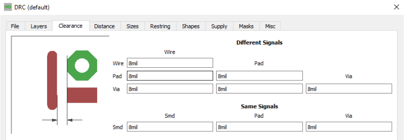
Get into the DRC by selecting ‘Tools’ -> ‘DRC in the board window. Something like this will pop up:

In the DRC window, you can set the minimum trace width for your project. The default is 8 mil, which is well within the capability of just about any board house. If you’re etching at home, you might want to bump this up a bit higher. For now, 8 mil separation is just fine, as are the rest of the default settings. Click through the tabs, and just see what options are available to you. There’s a ‘Check’ button at the bottom of this window. Click that, and you’re presented with all the errors you made.

When I ran the DRC on this project board, I had only one error relevant to this tutorial. The via I used to connect the VCC pin on the USB connector was too small. This drill was still well within the capabilities of OSHPark and Seeed, so I just clicked ‘Approve’. If your traces are too close together, or if they’re too close to a pad, the DRC will tell you.
It is imperative to run a DRC check before sending a board file off to a fab house. Not only will it help you stay within spec for the fab you are using, it will help catch silly errors that managed to get past you in the layout process.
Gerbers for Sending the PCB Off to Fab
If you’re only making two-layer boards and sending them off to OSHPark, Seeed, or DirtyPCBs, there is no need to do anything else to have your boards made. All of the usual online board houses accept Eagle .brd files. If you’re using any of these services, you can drag and drop your board file on the order page. It’s dead simple and almost foolproof.
 But the Eagle .brd file is not the industry-standard way of having a board fabricated. If you ever need a thousand PCBs, are making 6 (or more) layer PCBs, or just have some strange requirement, you’ll want to consider Advanced Circuits, Gold Phoenix, and numerous other options for fabrication. That means you’ll have to turn your board into a Zip archive full of Gerber files.
‘Gerbers’ are a collection of files that define each layer of the board. The top layer of copper is its own file, the top silkscreen layer is its own file, the top soldermask is its own file, and if you’re extremely good, Gerber allows you to create a layer telling a robot where to apply solder paste.
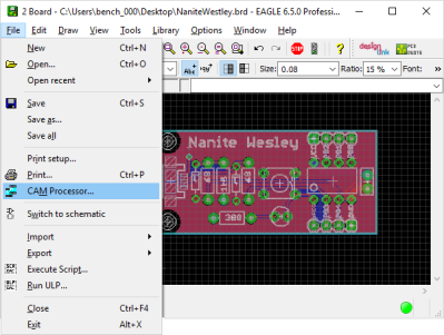
Lucky for you — and because this guide is already too long — OSH Park has a wonderful guide along with the CAM files required to generate Gerber Files. I highly suggest using OSH Park’s CAM file for generating Gerbers. It will generate the following files:
- Top Layer filename.GTL
- Top Solder Mask filename.GTS
- Top Silkscreen filename.GTO
- Bottom Layer filename.GBL
- Bottom Solder Mask filename.GBS
- Bottom Silk Screen filename.GBO
- Board Outline filename.GKO
- Drills filename.TXT
Put all of these files into a folder and Zip it up. Inspect your Gerbers with one of a dozen different online Gerber viewers. That’s really all you need to know about generating Gerber files from your Eagle boards.
That’s Eagle.
In several thousand words and three posts, we’ve gone over how to create a new, custom part in Eagle, draw a schematic, place those parts onto a board, draw traces, and send that board off to a fab. This is the bare minimum of an introduction to Eagle CAD. Now we can knock Eagle off the list of How To Create A PCB In Everything.
For the next few posts in this series, we’ll be taking a look at Fritzing. If you’ve been reading along with this series, you already know the right way to make a PCB in Eagle. Fritzing will teach you the wrong way. As always, we’re looking for suggestions on what pieces of software we should cover next. If you have an idea, leave a note in the comments.


I was hoping there would be a discussion on stencil files at this phase. Are there plans to address that topic in one of the next installments?
No. I’m done with Eagle and now I’m tearing my hair out at how much Fritzing sucks. It’s not hard, though. When you’re making the Gerbers, get another file for the tCream layer. That’s how you do that.
eagle is not done with you!
Ok, thanks.
The only stencil I’ve done to date was one where I manually edited the mask layer’s gerber file. I had created a simple PCB on circuits.io with a couple headers and SMDs, so its lack of support for stencils was more a learning hurdle than a technical one. Using the mask layer file, I just had to identify the through-hole sections in the gerber, remove them, then change the remaining SMD offsets slightly…
KiCAD is on my list of technologies to learn, though, so thanks for putting this series together. FWIW, I’d be ok with you skipping the Fritzing section…
Stencil files?
You mean paste mask gerbers, right?
They should pop out of the process right away.. I’m pretty sure Eagle still can do it as I did it 6-7 years ago for a small project.
When I had to do that again I looked at the EDA tools available currently and got stuck with KiCAD (open source, no cloud buy-in, files human readable).
Doing it for a year now and won’t look back.
Yes, paste mask is what I was talking about..
Thanks for the photo credit! :D. I see my photos all over the web, and I can count the number of credits given on one hand.
Sadly, you were credited on the only thing you’ve obviously messed up :) I would prefer to go without the credit on this one. On the other hand, kudos for sharing that picture with the world and making it better, as pretty much everyone has smiled when seeing the picture and said “Oh yes, I know this way too well!”
friends don’t let friends use fritzing
“What happens when you don’t run a DRC”… on eagle, i don’t think i could do that on kicad on purpose, it will not allow you to colide with other signals, on tracks and vias it will either shove or move around them (configurable), on pads it will simply deny going there
Nice you have mentioned DRC check. It is a simple step to perform but it is often disregarded (with catastrophic results, lol!!).
For anyone needing a programming fixture for your custom pcb check out my new open source project open fixture. https://github.com/ebuller/openfixture. Generates fully parametric laser cuttable dxf that can be assembled with m3 hardware.
That my friend is a cool project, I have literally no use for it right now but it makes me want to make something that needs it.
Hey, that’s pretty cool.
Thanks! It was built out of necessity (as many projects are). I kept revving the pcb of a product I’m working on. Every time I changed it the test points would move. Got tired of modeling and 3d printing fixtures so I came up with this solution. Let me know if you ever do use it! Would love feedback on how it works for other people so I can make improvements. Someday when I have spare cycles I’d like to push it into kicad scripting so it can be fully automated!
But, does eagle throw DRC errors for unrouted signals? Because quite some years ago when I used Eagle it didn’t. You could check using the ratsnest button how much unrouted signals there were, but that basically means that the DRC becomes a two-step process.
In my opinion, an unrouted signal should throw a DRC error.
Hi Marc,
This is a matter of contention. It is recommended that you constantly run DRC, that way you avoid going to far astray and ending up with 1000 drc errors at the end. Following this procedure, showing unrouted airwires in the DRC would be a tremendous pain since you would get a bunch of nuisance errors.
Historically, this has been the reason why unrouted signals aren’t shown in the DRC.
hth,
Jorge Garcia
Autodesk Support
Well, if you follow this philosopy it makes sense. I’m currently mainly a Kicad and Altium user. The online DRC in those packages makes sure that you at least don’t break the most common design rules. The offline DRC runs the more extensive checks and the errors from this check are usually easily solvable.
Maybe for Eagle an intermediate solution is to throw one DRC error saying “not all signals are routed”.
I hope that the input from Autodesk can help Eagle to improve, because I feel like it is falling behind a bit.
I have an almost embarrassing amount of faith in Autodesk’s ability to make Eagle awesome.
Thanks for the write-up Brian.
Hey – thanks for making all this so easy to follow. With the help of these articles I’ve ordered my first set of boards, and they’re due to arrive tomorrow!
Also – honestly – if fritzing is giving you a hard time, I don’t think we’ll mind if you skip it.
What about board edge connectors? I know there are lots of things that MUST be done for them, but I cannot understand them all :(