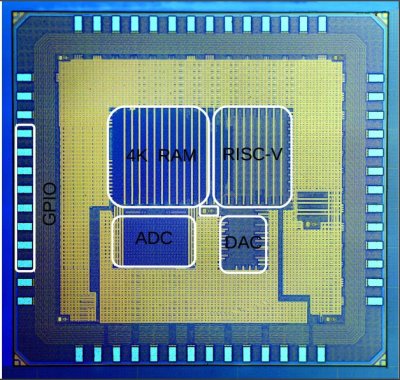
We don’t know about you, but the idea of an Arduino-class microprocessor board which uses completely open silicon is a pretty attractive prospect to us. That’s exactly [onchipUIS]’s stated goal. They’re part of a research group at the Universidad Industrial de Santander and have designed and taped out a RISCV implementation with Cortex M0-like characteristics.
The RISCV project has developed an open ISA (instruction set architecture) for modern 32-bit CPUs. More than 40 research groups and companies have now jumped on the project and are putting implementations together.
[onchipUIS] is one such project. And their twitter timeline shows the rapid progress they’ve been making recently.
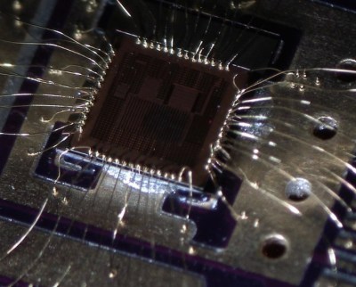
After tapeout, they started experimenting with their new wirebonding machine. Wirebonding, particularly manual bonding, on a novel platform is a process fraught with problems. Not only have [onchipUIS] successfully bonded their chip, but they’ve done so using a chip on board process where the die is directly bonded to a PCB. They used OSHPark boards and described the process on Twitter.
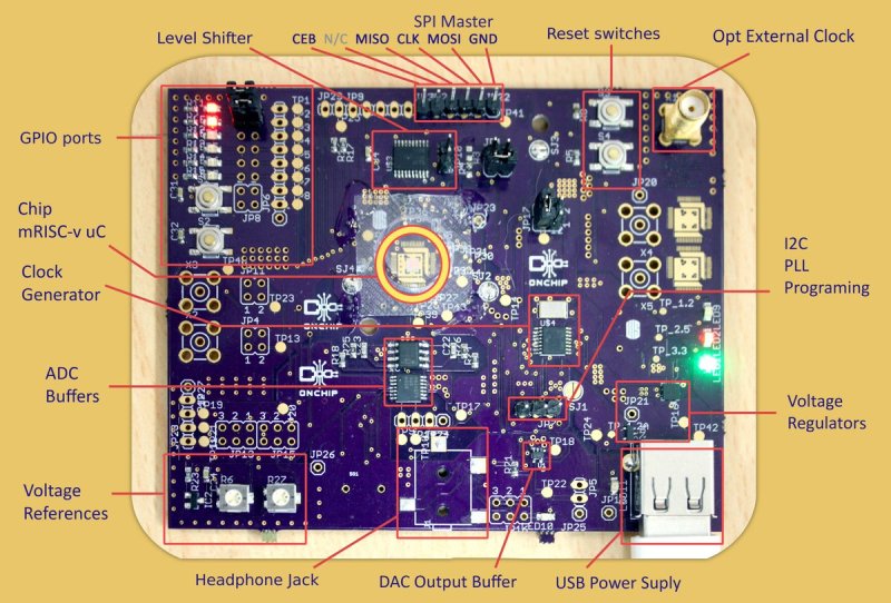
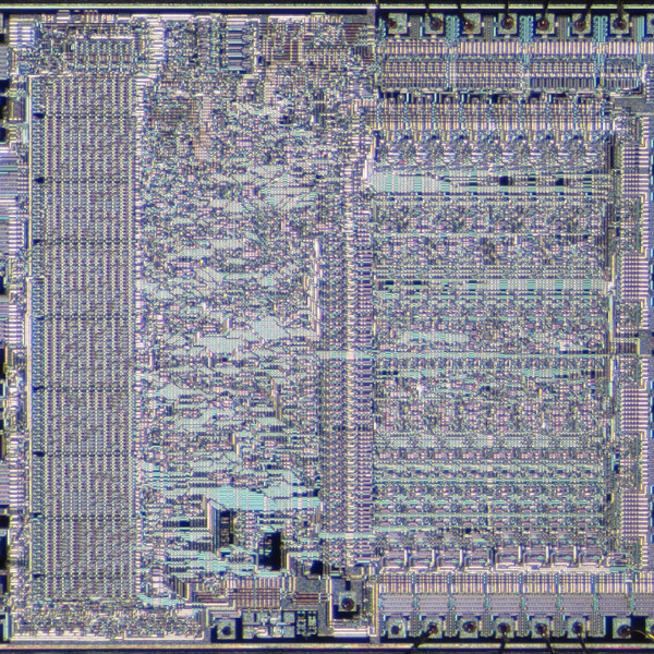
The board they’ve built breaks out all the chip’s peripherals, and is a convenient test setup to help them validate the platform. Check it, and some high resolution die images, out below. They’re also sending us a die to image using our electron microscope down at hackerfarm, and we look forward to the results!

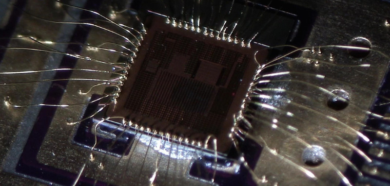





Ugliest wirebonding I’ve ever seen…..but absolutely astounding just the same! That they would go to such lengths is incredible.
True, they are ugly but considering that we still in the steeper slope of the curve of learning to wirebond, they work!
I don’t know for 17um gold wirebonds, it does not look too bad.
Scale: http://www.hastingsfilter.com/images/Micron%20Illustration.jpg
This is pretty awesome.
First, a little correction: RiscV itself is not (only) 32 bit, but 32, 64 and 128 (it’s a whole family of architectures, with an extensible instruction set: hot stuff).
Second: this is not alone. There are quite a few open/free processor architectures, some of them “out there”, e.g. Parallax Propeller (its VHDL files are released under GPLV3 no less), then there is OpenRisc (which actually lives as embedded implementation in several places) and last, but not least OpenRisc, which wants to be a free (64 bit) SoC based on RiscV (so peerhaps OnchipUIS’s bigger sister). They (OpenRisc) plan to have silicon “for the masses” some time this or next year.
Exciting times!
Yes, there was also OpenSPARC back in the day. Maybe you meant that by the first OpenRisc reference? https://en.wikipedia.org/wiki/OpenSPARC
No, OpenSPARC is yet another. I’m talking about or1k and family (which were, AFAIK, free design from their inception), cf. https://en.wikipedia.org/wiki/OpenRISC. But yes, some Sparcs have been “freed” by Sun before they were gobbled up, and there are, AFAIK free MIPS implementations too.
What’s exciting about the RiscV siblings (as this one and LowRISC are) is that the design itself is heavily used in academia for teaching (it was conceived exactly for that and is free of NDAs) and gets a ton of fresh mindshare. And is *now* breaking free of the virtual world of emulators and expensive FPGAs. Yay!
You could also use MIL-STD-1750A, the processor architecture designed by the US Army specifically to be implemented by multiple companies, in order to foster competition. Somewhat outdated (16-bit ISA), but you can also buy retail processors from manufacturers for testing etc.
https://en.wikipedia.org/wiki/MIL-STD-1750A
Used in space probes like ROSETTA, Cassini, etc!
“Cortex M0 RISCV”
Er, Cortex M0 is an ARM processor and entirely unrelated to RISCV (beyond ARM cores having RISC origins), not least that Cortex (in a processor context) is a registered trademark by ARM. I had a look back at the twitter feed but couldn’t see any reference to Cortex so not sure where this came from, was this a reference to the implementation of RISCV being similar to an ARM Cortex M0?
Yeah, it makes as much sense as saying “Intel Athlon 64” or even less…
Sorry typo. I meant to say… Cortex M0-like. I’ve updated the article to clarify this (it’s pretty much that class of microcontroller and this is mentioned in the EEtimes article I think?). Thanks for the note.
But surely it’s not like a Cortex M0, because it doesn’t have 16-bit instructions, and consequently, a similar level of code density?
In addition, one of the major reasons why Cortex M0(+) is competitive is because of the low gate count, with the CPU only having 12K NAND2 equivalent gates (roughly 24K transistors).
Doesn’t mean RISCV isn’t a good idea in its own right, but it doesn’t sound like a Cortex M0(+).
Having spent the money on custom silicon why would you cheap out on getting it packaged properly…?
I can’t say for sure, but I think it’s probably because academic money is weird.
They probably get free access to the fab facilities, but packaging is billed differently. Same goes for the wirebonder, might come off a grant (or go on the fab budget). But consumables? Might not be any money for that (actually personal communications with them also indicate that).
I’ve been in that position myself, it’s not uncommon in academia.
Nava you are right about some of the reasons:
1. MPW tapeout was covered not packaging
2. Packaging is costly due to NRE fee and with the money you spent 3 yrs in packaging you can buy a wb machine.
3. Logistics, we are in Colombia and shipping and customs are quite unpredictable. For instance some our chip have been for months in customs. You might imagine why
Technical reasons:
1. We need to get control over during test. We bond first few bonds and check and check and measure and measure
2. We need to have control of short wires (supplies). We push high speed stuff and more than 1mm length gives a pretty large inductance (2nH) when we are talking about 0.5ns ramps.
BTW, our uc is crunching with 1KHz to 200MHz clock.
Wow I didn’t realize you guys were pushing it to 200MHz already. That’s pretty awesome!
Wow 200….. I did the testing of our risc processor in our university group in the early nineties… I managed to get it up to 40 MHz…. Imagine what you can do with 20 years younger technology….
Last time I was involved in a tapeout in a large US company they dodge the customs by having someone carry the chips with him as hand luggage.
It would kind of make sense for that to be legal, because you can’t exactly import a shipping container that way, but…is it?
Maybe so they can change what they are probing without needing a new board?
What about tool support, though? Call me old and lazy, but gdb/openocd over a bit-banger isn’t my idea of fun, and Eclipse is a joke. It’ll need usable tools to compete – does it have them?
Please share your mind – what _is_ your idea of fun? I am using gdb/openOCD/Eclipse for daily stuff and it does the job for Cortex MCUs. It keeps me happy, perhaps because I simply don’t know better. I have another point of reference – Atmel Studio/proprietary debugging gizmo/AVR and it certainly feels no better (I’d pick the former any day).
Agreed! I’m a total noob when it comes to anything MCU, although I have a million and one dev boards here. Every time I start working on a new board, I subsequently end up with my MCU not doing what I thought I told it to do. And so every time, I fire up OpenOCD + gdb+tui, and within usually one or two hours, I know the root of the problem and can at least attempt a fix. And with me running Linux on almost everything I own, slow, buggy, MS-only software is not much of an option for me.
Frankly, using gdb’s TUI with OpenOCD as debugger is amazing. It may not have every bell and whistle out there (and support for some boards needs work), but it’s really easy to use once you’re accustomed to it.
My idea of fun is a quick, efficient, and featureful debugger. The interface to gdb is super-clunky, often painfully slow (e.g. watchpoints), and lacks the depth of hardware inspection provided by commercial debuggers (TLBs, cache dumps). It lacks the comprehensiveness required to debug the hardware, which will probably be a significant issue with an arch this fresh.
The closest gdb’s ever come to being faintly usable is with ddd on the front end – that barely works now due to the bitrot in motif, and even at its prime you were often left with a rats nest of data graphs.
Layering up open source may be great for getting a lowest common denominator feature set across all platforms, and giving hobbyists a new but ultimately useless toy. I’m interested in the tools for the SoC builders, the people who will take this core, and make it part of something truly special.
Like, like, like, an IoT hairdryer! … just imagine that, you’re on the other side of the planet and you want to use your built in hairdryer in your bathroom at home and you can turn it on with one swipe on your phone!
That would have been a killer idea during the 70s, but nowadays few people grow their hair that long.
Back on your jump-to-conclusions mat. This is first silicon of a relatively new architecture done by a university team.
And wot? Significant amounts of simulation should have been done before even thinking about synthesising some hardware. In industry, decent debugging tools are *exactly* how you bring-up fresh silicon.
The bonding to PCB is done to control the impedance of the bonds to ground and power connects to be able to go up to 200 MHz. This is not possible with standard packaging.
I like this for so many reasons (the most trivial is probably my favorite but I’ll leave that for the end):
It feels like there are fewer and fewer engineers involved in the actual silicon design with each passing year. Having open-source silicon opens a new vector for students and self-learners to study and learn the craft. This should lead to a wider pool of talented silicon designers which would catalyze better proprietary designs since new talent would come in with more experience than before.
I think widespread open IP for multi-purpose processors will push proprietary silicon developers to produce more new and interesting designs to stay ahead of the open IP.
The days of black-blob chip-on-board are over. Now the wafer is to be shown off like a jewel in the crown since the circuit doesn’t risk being stolen if not obsfucated. The wafers will be encased in a cover shown through the case like a watch crystal.
You do not want a see through cover over the device. Light will increase leakage of the semiconductor by creating electron hole pairs. For most simple designs the effect will be minimal but analog or low power digital circuits will seriously suffer.
Even open source silicon will still need opaque packaging to keep light from messing up the circuit. (see the the Pi3.) Every silicon junction is a little photo-voltaic or photo-conductive. Heck, I’ve used glass case switching diodes as (poor) photo-sensors.
I’m hopeful that the next 10 years sees custom silicon coming into the hobbyist space.
20 years ago a small PCB run was ungodly expensive, but now most of us would rather ship files off to OSH Park than pop the cork on the etchant. Low volume assembly is getting cheap too, and the proliferation of reflow toaster hacks and custom stencils has killed off rumors of the SMD apocalypse that has had hackers worried since I was a kid.
Thinking something like printable silicon where you can suck that hard… vacuum on a small chamber, where you’ve got your photo sensitive die and a DMD out of a DLP and you’re all pew pew pew with a laser and it craps out your own custom silicon…
… or you can just use FPGAs like a normal person. Think it will be quite a while before the price/benny doohickey looks bad for those…. especially as those seem to be gradually getting cheaper too.
There’s an idea! A grid of transistors, maybe a RAM chip or something similar. And you shine light from a DMD to customise it! The chip can feed back to the DMD somewhat itself, self-programming hardware! Live self-programming!
Okay perhaps there will be one or two practical implementation problems. But it’s an idea… certainly it’s an idea!
There are a lot of things you can never do in an FPGA, like properly clone a SID chip or make a low power SoC. And I’m pretty sure it’s a bad idea to run an ion implanter in your living room or keep tanks of arsine and phosphene hanging around.
Rocket lots are a thing, but they’re still way too pricey and involved for most hackers.
Short of building an NMOS fab, you’re never going to be able to clone a SID chip. The magic of the SID was from the intersection of the limitations of the process, and the vagaries of analogue semiconductors. Without that, it’s just a fairly boring, low resolution numerically controlled oscillator bank.
You still want to keep the silicon in the dark. We don’t cover chips in epoxy or metal just for looks, all those junctions are solar cells as well as diodes and transistors.
You are right about the junction concept getting energy from light, however the concept of having a translucent epoxy is the following:
1. Top layers are supply grids. Due to EM and IR drops, we covered most of chip with metals.
2. Although most of junctions are covered, is not fun to be able to check the effect of light in some blocks? We might see creative teenagers enabling new apps.
3. You can cover the translucent epoxy with some darkening tape, and taking it off when you want to show out to curious kids what is a chip.
4. We are looking for ways to excite and motivate kids to work on semiconductors. The current industry is lacking of new ideas.
You also want to protect the die from contamination and bond wires from mechanical damages.
As a guy who actually does silicon design for a living, I can tell you that this is not a field for hobbyists…
First, the actual tools to do the job are expensive! I mean “seven figures” expensive for a one-year license (you can haggle this down for buying lots of seats).
First, you need the simulation tools. These can be had cheaply — around the cost of a good used car. Next, you need the compiler (RTL to gates). This may be on the order of a good new sports car. Next, you need a place-and-route tool. Think about the cost of a decent house in a good medium-sized city. If you want an “advanced node” license for the smaller geometries, tack on another new sports car. You need a logical equivalence checker (used car prices, but you can probably safely skip this step). Power estimation tool — the good ones are once again in the “new sports car” price range. You also probably need a clock domain crossing checker — these look for design errors that are very hard to debug in real life, so I would want one. Maybe another used car price. Finally, you need a sign-off quality timing checker tool — perhaps the price of an average new (non-sports) car. At this point, your digital work is done.
Next, you need to do LVS and DRC checks, which typically run under an analog layout tool — yet another expensive (price of a house) tool. This also assumes that you are only doing digital design using standard cells and pre-made libraries. If you want to make your own custom cells, then you need spice simulators, and perhaps mixed-signal simulation tools — but I am not an analog guy so I am not as familiar with these.
OK. Now you have a tapeout (a bunch of files). Off to get them made! Depending upon the geometry, mask sets can be anywhere from a ten or twenty thousand dollars (very old, large geometries), all the way up to more than a million dollars (bleeding-edge “AMD,” “nVidia” and “Intel” type projects).
One way to reduce mask costs is to use a “MPW” — Multi-Project Wafer. In order to reduce mask cost, you share the mask with other parts or projects. Each mask is a “picture” of a layer of your chip, replicated as many times as you can within the area. However, instead of making multiple copies of your chip, the picture of your chip could be next to a picture of somebody else’s chip, or it could be 10 other projects, all on the same mask set. So, if you make a wafer, 10% of the die could be your part, and the other 90% could be other projects that get cut apart and sent to other people. This is fine for prototypes, where you only need a few wafers. However, for volume production, making 100,000 of your part may mean making 900,000 of other parts that you don’t want, which will drive up the cost.
Another money-saving trick is to use a “multi-layer reticle.” Your mask might have TWO layers on it. For layer 12, use the upper half of this mask, for layer 13, use the lower half. This cuts your mask cost in half, but makes manufacturing slower, as the mask is not effectively half the size, and thus needs to be exposed twice as much.
So, as you can see, making a chip, even for the older, larger geometries, is a VERY expensive game. In this project, it took a university to pull it off, so I am guessing that some EDA company (Synopsys or Cadence, for examaple) donated licenses for their tools. They might also have a relationship with a fab to get reduced-price wafers when the fab is in a slow period.
Still, if you just want to experiment with new architectures, there is nothing wrong with an FPGA — modern ones can compete pretty effectively on speed with older dedicated silicon, and the development tools are free or pretty darned cheap. Unless you are planning to need tens of thousands of these chips, or you really need lower power, it is hard to compete on price with an FPGA — even one costing a few hundred dollars, once you factor in the extreme cost of the tools and manpower of making custom silicon.
Maybe they’ve already done the FPGA bit, and perhaps use them for proposed changes. You wouldn’t, presumably, go to full fab without having debugged the thing. Still it says they got some special deals on the manufacturing.
There’s a lot of companies would be interested in this. Basically for the whole ARM market (or at least the lower-performance end to start with), but with no ARM IP, no licenses to pay or give a shit about. A lot of companies, I’m sure, would like to put some money into developing this. Particularly chip makers, since it’s they who pay the licensing fees. Same chip makers who charge so much, who have all the expensive hardware and software.
The Chinese went to the bother of inventing Loongson, so they’d have something they owned and could use on terms that suit them. That’s precedent for this, except this seems even more open and libre.
I dunno the special deal they got, but yeah it wouldn’t be sensible without it, to do all this at market rates. Perhaps the FPGA simulation is all done, and now they’re testing manufacturability, physical qualities, the sort of problems that crop up in actually manufacturing and using the real chip.
All that expensive software would be ripe for open-source alternatives to be made, although the market is a bit of a niche, I think. But if, like Mike says, this helps lead to an age where silicon design is something more people work with, and learn to do, there might be some drive to at least implement some alternatives to some of the expensive software. And from what you say, it seems like there’s plenty of opportunity. Open source has already provided revolutionary software alternatives to all sorts of previously horribly expensive stuff. The obvious one being a Unix alternative, Unix distros used to cost a fortune, with limited information available to their users. Powerful database engines another example. There’s plenty more obvious examples like that.
I think bringing the open philosophy to CPUs is a brilliant idea! Especially with the “management engine” backdoor shenanigans in popular CPUs now. There’s a lot of value in a true open core.
There is a lot to like about ARM, despite the license fees. There is a VERY deep amount of knowledge around ARM, and development/debug tools are plentiful — don’t forget how important this is. Still, if an open core could gain enough traction, that would be great! Inventing your own instruction set and CPU is actually not that hard. I could do it easily, if I were actually so inclined to do so. However, being a transistor guy, while I could make my own CPU easily, I could not create my own assembler/compiler nearly as easily, and porting GCC to my own invention is also beyond my capabilities.
If you are willing to eat your own dog food, a company could easily make their own processor and compiler, However, that is a tougher sell when trying to sell to customers. A customer can use something that they know, have experience with, and already have tools for, or they can use something brand new. Maybe this can eventually be overcome, but it will be a tough sell.
A completely open CPU is certainly a cool idea, and I hope that it takes off. However, “testing manufacturability” is not really a thing. Assuming that they used standard cells, the fabs KNOW about the manufacturability of their process. An “and” gate is an “and” gate, and fabs have a good handle on how many defects happen on an average wafer. The only time you really NEED to test silicon performance is if you are making your own custom blocks (oscillators, PLLs, SERDES, A/D converters, voltage regulators, etc.), and this is assuming that you can’t use a pre-made library.
I think that more open hardware would be great, but I just don’t think that the economics make sense. A mask set for 65nm may run on the order of hundreds of thousands of dollars (just my fuzzy memory, since I never actually deal with the financial aspect). Mask sets for much older geometries may only be in the tens of thousands of dollars, so that might be possible for a smaller company or a VERY popular Kickstarter, but certainly not for a lone engineer in his basement.
There actually are a couple of open-source free chip design out there, but I have no experience with them. With mask sets being so expensive, and time-to-market being critical, it makes no sense for a company to take risks. If you save $2,000,000 on tools, but make a chip that does not work, and your competitors beat you to the market, what have you really gained?
Hi Kevin, what a great summary explaining tools costs and some digital methodology. I do agree with you that the current state of silicon design is not for hobbyists. However, you might are not seeing the big picture. We have also been in the industry, and let me give you the following insights based in your comments:
1. Most of IC designers whom I have worked with are pretty unsatisfied with the state of tools and methodologies. We need a bunch of people that can change this. Remember that Content management systems were produced sometime ago for a couple of companies, now check the state. Two EDA companies have consolidated but there is a lot room to improve.
2. Tools have been incremental.A current PnR tool for instance, is a series of patches of acquired features with time. By just rewriting them from scratch will help. For instance, from Encounter to Innovus.
3. EDA industry is matured enough but its tools are far from what they should be at 2016. It s just a matter of time for a a skilled kid in some corner of the world, that has been motivated, to crack EDA problems.
4. New algorithms showing up at DAC and ICCAD are improving performance of EDA tools but they take about 2 to 3 yrs to be implemented in commercial flows due to the inertia of EDA companies. Again, a lot of room there.
In general, what I am trying to say is that to build a house you need the first bricks. We are trying to excite programmers, hackers, hobbyists and makers to look at the possible perspective of having open silicon chips in he long and midterm term future. Imagine how many new apps, new tools, new circuits and new architectures may appear if the critical mass increase considerably!
For a possible crow-funding campaign, we are thinking in using the Adapteva approach to get use of commercial tools as minimum (time and number) by adapting open-source tools and use paid tools just as necessary. As a school we are not allowed to extract economic benefits.
As a prediction, For 2024 there will be an available open-source tool capable of doing smarter and faster PnR without the need of too many knobs to get a close-optimal place-and-routed chip. Similar case: webservers, recall IBM and HP webserves, now open-source based dominates.
Well, I wish you all the best luck in the world! I hope that you succeed!
It would be cool if silicon manufacturing were actually more accessible. I could imagine a fab dedicated to hobbyists. Perhaps with a combination of multi-project-wafers, multi-layer-reticles, and blind-building (no testing), then silicon might become actually affordable — maybe only $10,000 or $20,000 for a few prototypes! This would necessarily be limited to older, larger geometries, but that would still be awesome. However, this would also require some good, free libraries.
Maybe packaging would be simplified by having a number of “standard” footprints. Make your die this size, and put your pads here, and we will package them in this standard package.
I don’t know the situation with advanced nodes, but for older processes those EDA companies must be making out like bandits. The basic problems you describe (DRC, crude timing simulations) are not that difficult, FOSS tools for it have existed for decades, and internal ones have been done by many companies (I worked on some). If you look at greenarrays.com, that’s a 144-processor chip designed completely with in-house tools written in Forth! (It’s a Forth CPU, too). They did several MOSIS (MPW) prototype runs at around $12K a run, and then a couple of production runs (cost unknown but almost definitely no higher than low six figures). My old company had several internal fabs (not anywhere near “advanced” even for that era) and getting experimental chips made (designed with our internal tools) was not that big a deal. I suspect it cost a few K$ on the fab side to make a chip but we were encouraged to do it even for hobby-type projects, to build up our skills and experience. This type of thing has also generally been available to EE grad students working in VLSI-related areas. I like to hope it will get more accessible rather than less.
I hate to reply to myself, but one thing that I completely forgot to mention in the standard ASIC flow — testability.
Once your design is done, you have to make sure that you only ship working parts, so you have to insert scan into the design. This is a system that allows all of the basic logic gates to be tested. This is usually done by the synthesis tools as a separate phase and in a separate mode (with a separate license). “Scan chains” are created and hooked up.
Then, once the design is done, you use another tool (yet another expensive license) that creates test patterns to exercise all of the logic. Once a wafer is made, each die is tested with this pattern, and allows faulty chips to be identified and discarded.
There were some pretty decent free tools for VLSI design, back when I was teaching it 30 years ago. (I’m thinking of the MAGIC layout software from Berkeley, for example.) From what I’ve heard from industrial VLSI designers, the industrial CAD tools have not advanced much beyond that in the last 30 years.
MOSIS (https://www.mosis.com/) is still providing fairly low-cost multi-project wafers for university projects.
Here are some improvement just off of the top of my head…
UPF (Universal Power Format) lets you specify voltage islands, where different blocks use different voltages, power off blocks, etc. This is a HUGE deal, as it automated level shifters and retention cells.
SystemVerilog has some goodies for RTL.
** Compilation **
Register re-timing.
Clock gating.
** Place and Route
Multiple voltage threshold (reduce leakage current)
Useful Skew
Litho-Friendly Design (yes, you might actually want a yield over 10% at 16nm)
Wow – it’s not much that impress me in open Source, but this one does. I am actually looking forward to the day I can get my hands on one of these.
I wonder if some day some great hacker will bring silicon fabs to our garages just like they did with 3D printing. Could you imagine designing and building your own custom chips or even using open source chips like the one above but changing it to fit your needs. I know we have FPGA but will we ever have our own fab labs?
No. Will never happen due to the expense of the machines. 3D Printing was held back by patents not expensive machines. FDM has always been done with low-grade cartesian bots.
Silicon fabrication is a whole different ball game, not to mention the use of hydrofluoric acid etc.
This is so fricking awesome! Do a kickstarter! I’ll buy a board! Maybe you can get other groups involved as well, maybe in the US so that you free yourselves a bit from the Colombian bureaucracy.
I guess the idea of developing this kind of tech in Colombia goes beyond the Colombian bureaucracy, it’s more about letting the world know that tech is a deal in Latin America as well. Nonetheless, that’d be superb to set up a Think Tank alongside the funding in order to achieve the project’s goals.
I guess the idea of developing this kind of tech in Colombia goes beyond the Colombian bureaucracy. It’s more like letting the world know that tech is a deal in Latin America as well. Nonetheless, it’d be superb to set up a think tank alongside the funding in order to achieve the project’s goals.
I’m hoping that we’ll eventually see high performance OS SoCs like the ones that permeate the phone/tablet/etc market with GPUs and all so that we can get true longevity out of devices. No more binary blobs that get 0 support after the device ships.
Well, seems they got quite a bit further than the old “Freedom CPU” project.
Working on a new chip is one of the most fun one can have, finding out max clocks, adc and dac speed & drift, latency, finding bugs, thermal effects exc
is possible to integrate it with parallela.org ?