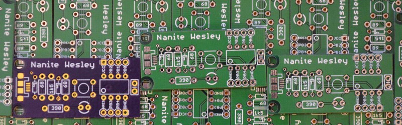
This week, we’re continuing our Creating A PCB In Everything series, where we go through the steps to create a simple, barebones PCB in different EDA suites. We’re done with Eagle, and now it’s time to move onto Fritzing.
![]() Fritzing came out of the Interaction Design Lab at the University of Applied Sciences of Potsdam in 2007 as a project initiated by Professor Reto Wettach, André Knörig and Zach Eveland. It is frequently compared to Processing, Wiring, or Arduino in that it provides an easy way for artists, creatives, or ‘makers’ to dip their toes into the waters of PCB design.
Fritzing came out of the Interaction Design Lab at the University of Applied Sciences of Potsdam in 2007 as a project initiated by Professor Reto Wettach, André Knörig and Zach Eveland. It is frequently compared to Processing, Wiring, or Arduino in that it provides an easy way for artists, creatives, or ‘makers’ to dip their toes into the waters of PCB design.
I feel it is necessary to contextualize Fritzing in the space of ‘maker movement’, DIY electronics, and the last decade of Hackaday. Simply by virtue of being an editor for Hackaday, I have seen thousands of homebrew PCBs, and tens of thousands of amateur and hobbyist electronics projects. Despite what the Fritzing’s Wikipedia talk page claims, Fritzing is an important piece of software. The story of the ‘maker movement’ – however ill-defined that phrase is – cannot be told without mentioning Fritzing. It was the inspiration for CircuitLab, and the Fritzing influence can easily be seen in Autodesk’s 123D Circuits.
Just because a piece of software is important doesn’t mean it’s good. I am, perhaps, the world’s leading expert at assessing poorly designed and just plain shitty PCBs. You may scoff at this, but think about it: simply due to my vocation, I look at a lot of PCBs made by amateurs. EE professors, TAs, or Chris Gammell might beat me on volume, but they’re only looking at boards made by students using one tool. I see amateur boards built in every tool, and without exception, the worst are always designed in Fritzing. It should be unacceptable that I can even tell they’re designed in Fritzing.
Fritzing has its place, and that place is building graphical representations for breadboard circuits. Fritzing has no other equal in this respect, and for this purpose, it’s an excellent tool. You can also make a PCB in Fritzing, and here things aren’t as great. I want to do Fritzing for this Creating A PCB In Everything series only to demonstrate how bad PCB design can be.
For the next few thousand words, I am going to combine a tutorial for Fritzing with a review of Fritzing. Fritzing is an important piece of software, if only for being a great way to create graphics of breadboard circuits. As a PCB design tool, it’s lacking; creating parts from scratch is far too hard, and there’s no way to get around the grid snap tool. No one should ever be forced to create a PCB in Fritzing, but it does have its own very limited place.
Not Making A Part In Fritzing
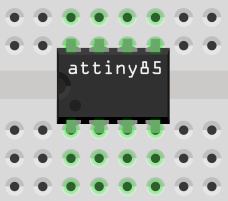
As with all tutorials in this Making A PCB series, I would like to start off by making a part, specifically an ATtiny85. Does Fritzing come with an ATtiny85? Yes, it does, but that’s not the point. You do not know how to use a PCB design tool unless you know how to make a part for yourself — what you own owns you, self-sufficiency, and all that jazz. It’s the mindset required for any hacker or maker philosophy, and necessary for anything that bills itself as an engineering tool, because sometimes you are the first person to use a particular part.
You cannot create completely new parts in Fritzing. This is from a blog post highlighting the new Parts Editor released in version 0.7.9. Packages can be edited into new parts, and most jellybean components have drop-down menus for different values; in the parts library, the through-hole resistor is a 220 Ω, but there’s a drop-down menu for the most common values you’ll need.
Of course, you can create new parts in Fritzing, and that blog post saying you can’t is an oversimplification. The parts already in the Fritzing library got there somewhere, but recreating the efforts of the devs is a pain. First, you need to download Inkscape, draw your package with pins and pads and text on an unreasonable number of layers. Save that as an SVG, go into Fritzing, edit an existing package, do the macarena, sacrifice a goat on the night of the blood moon, and eventually, you’ll have your completely custom Fritzing part. This is unnecessarily complex for any EDA suite.
I will not be demonstrating how to make a part in Fritzing. It’s far too much effort for far too little payoff. No one should use Fritzing to create a PCB, anyway, much less create their own parts from scratch.
Step 1: Create Your Board On A Breadboard
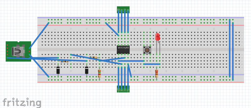
There are three steps to creating a PCB in Fritzing. The first is to create a breadboard circuit, the second is to turn that into a schematic, and the last is turning that schematic into a board. This is simple enough, the search function works, and the circuit we’re building can be easily built on a breadboard.
It’s important to note this skeuomorphic design pattern shouldn’t be taken too literally. You can build things in Fritzing with an Arduino or Raspberry Pi, but neither of these are breadboard friendly. Here, you need to drop things off to the side of the solderless breadboard and run a few wires. That’s what I did with my USB port here.
Step 2: The schematic
At the beginning of every school year, first-year engineering students are rounded up into a lecture hall for an introduction to the program. Around the end of this lecture, the head of the department walks up to the podium and says, “Look to your left, look to your right, one of you will not make it to graduation.” Fritzing sat between two mirrors. The following schematic says it all:
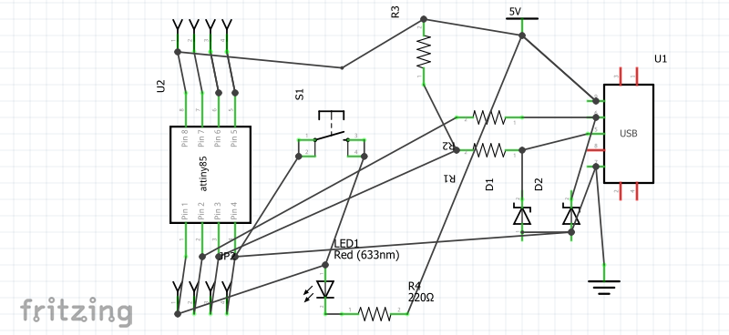
 There are no nets and no busses in the Fritzing schematic view. The only way to connect parts together is by connecting individual pins together. You can’t name connections like you can in Eagle, or in any other EDA suite. This is the bare minimum of what schematic design can be. It can be done, but it’s not done well.
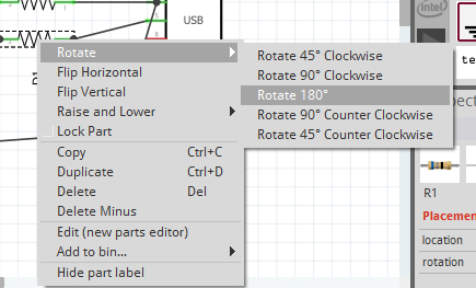
One of the more annoying unfeatures I found was the inability to rotate a part by right clicking. To rotate a part in Fritzing, you need to go through a contextual menu. This is horrifying and seriously cuts down on productivity.
Fritzing’s schematic design philosophy is based on wires connecting two pins, instead of nets between pins. Try to ‘tap into’ a wire in the schematic view in Fritzing. You can’t, unlike every other schematic capture application on the planet. In comparison, Fritzing’s schematics are terrible.
Step 3: Making A PCB
This is the meat of this post. No one needs to know how to connect parts together on a physical breadboard and a bunch of wires. The breadboard interface makes sense – it should, anyway, since the greatest use case for Fritzing is creating graphics of breadboard layouts. The schematic is ugly, but it “works”. Now it’s time to actually build a board in Fritzing. What does that look like?
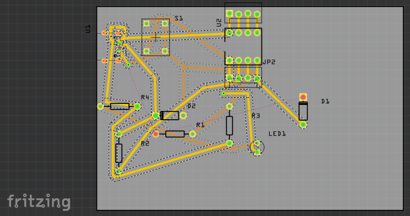
Putting the obvious aside, let’s go over what we actually have here. In Fritzing, you can make a two-layer board. The color for the top layer is yellow, the color for the bottom layer is… darker yellow. Several board outlines are included, from a resizable rectangle to Arduino and Raspberry Pi shields (a neat feature!). Holes are possible, and despite what nearly every PCB made in Fritzing says otherwise, traces with a width smaller than 24 mil are possible. This is important because the micro USB port we’re using is unusable with 24 mil traces.
There are a few cool features to the Fritzing PCB mode. Nets are color-coded, for instance, which would be welcome in any piece of software intended to build PCBs. There are shortcomings, though. Copper pours are separated into two categories: ground fills and copper fills. What’s the difference between these two? Ground fills may only be applied to ground signals. Copper fills can be applied to any signal. It doesn’t take expert knowledge of PCB design to see this distinction is arbitrary; all a copper/ground fill does is draw a polygon, fill that with copper, and connect the relevant pads. There is no way to define the shape of this polygon in Fritzing. This is harder than it needs to be.
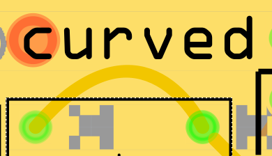 One frequently repeated falsehood concerning Fritzing is that it is fundamentally incapable of doing curved traces; that’s why all boards made by Fritzing look terrible. This is not true. You can curve a trace by holding CRTL while dragging it. In fact, a lot of what makes PCBs made in Fritzing look bad can be corrected by pressing either CTRL or Shift while dragging a trace. Traces snap to 90° if you hold down Shift.
Of course, there are problems. Vias, or running a trace from one layer to another, is unnecessarily hard. I would rather use any other EDA suite except for Fritzing, but you can make a board in it. Check it:
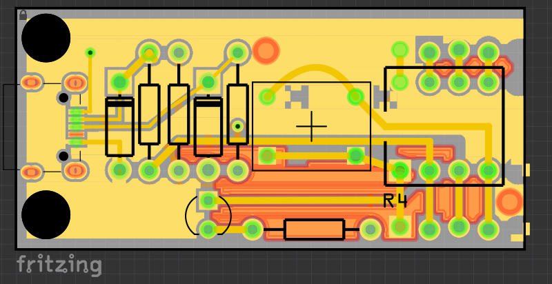
Does it work? Yes, probably. If that’s the measure of a success, Fritzing is an acceptable PCB design tool. I’m a little more particular, and like usability in my tools.
Turning A Fritzing Board Into A PCB.
Right at the bottom of the screen, you can find a ‘Fabricate’ button that will send your board to a fab house in Berlin. The cost for my board is €6.26 for one. Of course, you can export a Fritzing board as a Gerber, and send that off to any fab house on the planet. For my board, OSH Park will give me three for $7.15. I could get ten of these boards made by the Fritzing fab for €55.44, but I already bought twenty of them for $36.29 from Seeed Studio.
Is Fritzing a good PCB design tool? No, no it’s not, and friends don’t let friends use Fritzing. If you have zero money, but still want to design a board, Eagle is free. Making parts in Eagle is easier, and there’s a link to a really great guide below. KiCad is also free (speech and beer), and and you can literally design anything with it. There are better options.
Fritzing has a place, though, and that’s making graphics for your Medium blog on how you made a Raspberry-Pi-powered weather station. Here, Fritzing excels. It has everything you need, a relatively simple user interface, and makes great graphics. Friends don’t let friends use Fritzing for PCB work, but if you need a graphic of a breadboard layout, I haven’t seen anything better.


Hackaday articles really need a brief paragraph describing the purpose of the article. These titles mean nothing.
Good idea. I recommend something like this:
“This week, we’re continuing our Creating A PCB In Everything series, where we go through the steps to create a simple, barebones PCB in different EDA suites. We’re done with Eagle, and now it’s time to move onto Fritzing.”
I will now go back in time, hack the site and insert it as the first paragraph of the article.
The Haxor is strong in this one.
Thank you. I have NO IDEA what all that text in the article was about. Now I do. I think. If it was meant to paint Fritz(-ing) in a good light, it did not succeed.
It was meant to highlight the good and bad features of a commonly used package used for PCB design. Folks here are more concerned with utility. Making it look good is up to the advertisers.
yes, actually, it did. about the best light you can ever put on fritzing PCBs.
The “friends don’t let friends” thing is an American idiom. I think originally referring to some prohibited drug or other. In this sense it means “Fritzing is bad”. That came across from the title, and pretty accurately described the article. With the exception that “Fritzing is good for drawing breadboard layouts” (which I think is it’s actual intended purpose). So the title fit the article fairly well.
As for Fritzing’s lack of PCB ability, I suppose that ability was glued on later, and they haven’t done a good job of implementing it yet. An electrical circuit can be described equally accurately as a circuit diagram, breadboard, or PCB, the information’s interchangeable. So it should be possible to get it up to scratch given time.
You got it. The original was “Friends don’t let friends drink and drive”. It’s been rolled into many things over the years.
“Look to your left, look to your right, one of you will not make it to graduation.” Fritzing sat between two mirrors. That was the funniest thing I’ve read in awhile.
Absolutely!
Will these series be doing a quick “How to get started in KiCAD” article? I was looking forward to being done with the Eagle articles. But this one was next.. I didn’t even know Fritzing did PCB stuff. But after reading this, I would still claim that it doesn’t.
We’re doing a KiCad one, at least as extensive as Eagle.
I’m not rushing it, because people would just stop reading after KiCad. There’s a lot more I want to do with this series. Next one, I think, is going to be AutoTraxx as a ‘historical’ look at PCB design.
So you’re going to do kicad last because its the only one people actually want….sigh….
I know, right? Free shit is the worst. ESPECIALLY when you have to wait for it.
I’m especially looking forward to the One Secret Tip For Helping You Not Delete KiCad After 5 Minutes Of User Interface Frustration.
The secret tricks I know for kicad (pcbnew) are:
-F11 enables OpenGL mode, which has all the cool new stuff
-When placing traces, ‘E’ brings up the settings for the interactive router, which has walk around and push & shove settings
-‘D’ drags a segment without disconnecting it and keeps the slope of the adjacent segments
Knowing this from the beginning would have saved me quite some frustration, but now I’m really happy with kicad.
Meanwhile try: https://www.youtube.com/playlist?list=PLy2022BX6Eso532xqrUxDT1u2p4VVsg-q
^ This!!!
You can always drop by on KiCAD.info and ask for help if you got problems with KiCAD.
We’re a quite handsome bunch.
Don’t forget to add the info about the Eagle to KiCad migration/emancipation path.
In the mean time there is the following on Kicad’s website:
http://docs.kicad-pcb.org/stable/en/getting_started_in_kicad.html
That was enough to get me started.
Thanks Brian, now I’m scarred for life after seeing that schematic photo. Let the nightmares begin.
Worth mentioning that the raw components within Fritzing are available as SVG, meaning you can step outside Fritzing and use Inkscape or your favourite proprietary vector editor to work around issues of scaling, obscuring or visual elegance. This is an approach we have used at http://shrimping.it A LOT, such as the Blink Arduino-compatible build… http://start.shrimping.it/project/blink/build.html
While i agree withsome of the comments. I can and have made plenty if working pcbs with fritzing but i still can’t work out either kicad or eagle
For a casual PCB designer (2 or 3 a year) Fritzing is perfect, I don’t have the time to learn new PCB design software just so I don’t have to use Fritzing which for the dozen or so PCB’s I’ve designed and purchased over the last few years all work perfectly, I used Eagle before I tried Fritzing and appreciate Eagle is a better more advanced tool for PCB design but Fritzing is just quicker and easier to get a working fabricated PCB in your hands.
If free, rather than open, is sufficient, give DesignSpark a try. I was pleasantly surprised by how the UI elements operated in a similar manner to how they do in every other class of application. Part creation’s a snap, which addresses the main complaint I had about Fritzing.
Altium user here — I had to use Fritzing for sake of a client that could barely handle the idea of using anything more sophisticated. Just out of curiosity, I used the PCB tool. Coming from Altium to Fritzing, I could find all sorts of faults with Fritzing without trying. But I’ll say one thing — it was super easy to make an arduino shield with Fritzing’s pre-existing pieces for a relatively simple project. Would I use it for myself? Hell no. But If someone has a bread-boarded project with some basic R’s, C’s, LED’s, and a few I/O’s, Fritzing is actually not a bad low-learning-curve introduction to the benefits of getting a 2-layer board made… Just don’t stay there.
i agree. fritzing is good for starters. you can make your own parts of others have said before. i really don’t think it tries to compete with eagle or kicad. the low learning curve (as opposed to eagle and kicad) make the program useful for beginners.
I was expecting an impartial, fair, detailed and useful article about this software. I got Brian Benchoff instead.
Reward: $100 to the first person to make and document a DIP ‘tiny85 part *from scratch* in the current version of fritzing, as complete as the most anal hackaday commenter would expect, posted to hackaday.io. I’m serious.
Fritzing is fundamentally flawed, and I have no obligation to be fair to something that is inherently bad.
> Fritzing is fundamentally flawed, and I have no obligation to be fair to something that is inherently bad.
That’s what Hitler said.
One person was talking about a piece of software. The other was talking about a people. You think you’re being rational to compare the two?
You seem to be the kind of delusional fritzing fanboy. You should spend the effort learning a better tool instead of arguing so much about a bad tool.
Out of curiosity how much does Hackaday pay for such an article, on average? $100 seems like a bad deal.
There are zero guides to creating a part from scratch in Fritzing, documentation is important, and any open source/open hardware culture depends upon documentation, but $100 isn’t enough to help the community.
See? By your logic, I can’t pay someone to get people using Fritzing. Fritzing sucks that bad.
By your logic, you didn’t do it even when you got paid for it, and now you are trying to, um, delegate.
Here is a list of guides: http://fritzing.org/learning/tutorials/creating-custom-parts/
No Inkscape required, you can do it all in vi if you like. I made several Fritzing parts from scratch, since I´m too stupid to use Eagle. For most designs I don´t bother and just use some manually placed pads though.
@Daniel:
> Creating custom parts using the Part Editor
> We released a new parts editor in version 0.7.9 of Fritzing, so these tutorials are currently out of date.
I’m hearing a lot of, “it’s easy” and not enough, “here’s how you do it”.
> I’m hearing a lot of, “it’s easy” and not enough, “here’s how you do it”.
The linked page links to six tutorials explaining in detail how to make a new part from scratch. One would be enough “here’s how you do it” in my opinion…
There already is a ‘tiny85 part.
Mattia Francesco Moro made it back in 2012.
https://github.com/fritzing/fritzing-parts/blob/master/core/ATtiny85.fzp
“as complete as the most anal hackaday commenter would expect”
Add some zeros to the end of your bounty figure, then, and not after the decimal point, either.
“fundamentally flawed… inherently bad”
Ever heard of constructive criticism?
(And I say this as someone who successfully used Fritzing for precisely one board, who recognises its weaknesses, and who has now moved on to KiCad, so I don’t feel the need to defend the project other than to say that it’s as much in your power to make it better as it is those who developed it. And at least they aren’t trying to exploit you, unlike certain proprietary tool vendors. Well, unless you think that Fritzing Fab has made the Fritzing people millionaires through outrageous mark-ups on that notoriously super-cheap German labour involved in getting all those vitally important ATmega boards made.)
A impartial, fair and useful article about Fritzing will tell you that Fritzing is awful. I don’t see where this failed to do that.
This series by Benchoff is inhrently flawed IMHO. There is so-much investment when learning and using most pcb packages that a substantial bias is inevitable. Benchoff’s bias shows I think in his recommendation of using Eagle.
Immediately when using one that “is not your normal” you will throw your hands up and say things don’t work, not because they don’t work but because they don’t work the same way as your normal package does.
In the case of Fritzing it is even worse, because you are not making a fair comparison at all, Fritzing is not designed for competing with DipTrace, or CircuitStudio, or kiCad or… it is a fundamentally simpler system for people who have never before done any circuit or pcb design to get started, intuitively, easily, with no in-knowledge.
The complaint about named nets is a prime example, not only IMHO does somebody who knows nothing not need to use named nets, they should not use named nets, it just confuses the situation and can lead to very bad habits (“wireless schematics”, we have all seen them).
As for Benchoff’s attempt at a schematic, if that was done by Benchoff I can only assume it was deliberatly drawn like this to make things look bad, or “didn’t work like eagle, screw it”. It’s been a while since I’ve used Fritzing, but it’s entirely possible to make your schematic look presentable, for the audience with which Fritzing is intended.
With that said, while Fritzing is an excellent introductory learning tool, it doesn’t take long before you outgrow it’s ability, add to that the effective inactive development over the last couple years and it’s just kinda hanging in there. DipTrace is IMHO the natural progression, for it’s similar intuitive nature (but again, people with preconceived notions, should leave thier baggage at the door).
Additional, Benchoff makes it sound like you *have* to start with a breadboard, that is no
[…stupid tablets touch screens and no edit comment] (starting in breadboard) that is not correct, you can use bb, sch and pcb in any order, updates to any will propogate to the others.
Much like smart TVs it’s an oxymoron.
I looked briefly at Fritzing as a simpler alternative to Kicad for some projects. Their own tutorial has you start by drawing a breadboard, and this is what turned me away. Since when is the breadboard a starting point for anything? Rendering a breadboard implementation is a way of taking a schematic and turning it into something that somebody who can’t read schematics can use to build something. Any sensible person starts with a schematic, and if you’re building the project yourself, it’s quicker to build the breadboard than it is to draw the breadboard and then duplicate it.
I agree on this. It would have been better if they’d switched the tab order to schematic, breadboard, pcb, IMHO.
As I say, it’s just UI as there is nothing preventing you starting in sch (and I never actually used the breadboard tab at all).
“Since when is the breadboard a starting point for anything? ”
Never?
Breadboarding (using a wooden board for cutting bread to assemble a test circuit) is not a starting point, it is done after you have drawn up your schematic on the back of the tavern napkin.
So, before I would start to breadboard something, I already have a schematic.
So after I have a scheme, then it is time to fire up the CAD software.
I like Diptrace (after giving up on Eagle and KiCAD), but I still really hate its library layout. A giant list of part numbers without manufacturer for everything, including connectors? Time to play “guess the intersection of the TE Connectivity catalog and the Diptrace library”…
There are net labels in schematic view in the core library
I have used them and they work well. I did design my own esp8266 sensor node in Fritzing and I could make do. Still have to send them off for manufacturing..
I agree Fritzing is not the perfect tool for everyone, and it has its problems. But those are not the problems described in this article. It also has a lot of bright points, the most important for me are:
* You can start with the PCB. You can start in any of the views, in fact, do some work, switch to other view, make some changes, switch again, make some corrections, etc. — and a lot of work has been put to make it work well. This is especially important for me when I don’t start with a ready schematic, but instead make it up as I got. For instance, I don’t care which servo is connected to which GPIO pin in my robots, as long as each one gets its own pin. So I start with the PCB view, and connect the servo headers with the pins based on what is the easiest to route — and then switch to the schematic view and make the connections.
* The breadboard view is not only for the breadboards, and in fact, it’s not where it actually shines. You can delete the breadboard and instead drag one of several available proto-boards in there. Then you can very easily arrange all your components (since you see the physical shapes and sizes), break the strips on your strip-board by clicking on them, add wires and design your prototype.
* It uses a familiar, modern GUI paradigm. Just drag-and-drop things where you want them. No need to press some strange key combination while holding your mouse in exactly the right place, no need to switch between a hundred tools and modes, no way to put your traces on your soldermask layer, etc. And you can also tell at a glance what you are looking at.
* It’s a great shame that there is no description of making a part for Fritzing, because I believe that’s where the editor really shines in comparison to the alternatives. Instead of a primitive, ad-hoc, keyboard-controlled “editor”, Fritzing lets you use any vector editor of your choice, whatever you find the most convenient. Of course, you have to know how to use the editor you have chosen, which certainly may be a barrier for some people, but if you know how to use it, you get a really powerful tool in your hands. In addition, I think that Fritzing is the only of the bunch that actually uses open standards and formats, which would make it a great feature, if only any other tool decided to do that, instead of inventing their own broken formats. Once you have the footprint for your part drawn (usually copied from the datasheet and adjusted to the right dimensions), you just group the elements by type (pads, labels, outlines, etc.) and label them, so that Fritzing knows what is what. Then you edit a part that looks similar to what you need, import the image, label all the connections, save it and you are good to go. No, you don’t have to draw the element’s physical looks if all you need is a footprint and a schematic symbol.
* In the recent version, you have the option of saving the designs and the parts in an uncompressed format, which is great if you, like me, like to keep your designs in a code repository, together with the rest of your project.
* You can export your designs as images (raster and vector), pdfs, gerbers, and pretty much anything you like. No jumping through hoops just to get your work in an usable format. You can easily share the images of your design in your build logs, print the pdfs for home etching, or send the gerbers to a fab house. I have never used the “order” button in Fritzing myself, so I can’t comment on the quality of what you get, but as I understand it’s slightly expensive mostly because you actually get your design reviewed by a professional before fabricating.
As I said, Fritzing has its own problems too, and the most important for me are:
* Rectangle selection selects everything that the rectangle touches, usually including your PCB, not just the part you meant to select. It would work much better if it instead worked like Inkscape, and only selected the parts that fit inside the rectangle whole.
* It is sometimes difficult to click on the thing you want to click on, especially if there are a lot of overlapping layers of them visible. There is some layer management (send to back, bring to front, etc.), but it’s a bit of a pain and doesn’t always do what you expect. I learned that the easiest way is usually to just move the obscuring part away, do what you need, and then move it back in place.
* The bulk editing capabilities are pretty much limited to moving stuff around and maybe rotating it. You can even move several selected parts to the bottom layer easily — you have to move each one separately. The same applies to editing the component’s properties, such as the diameter of the hole for a pin header — you have to tediously repeat it for each part. That makes Fritzing unsuitable for larger designs with a lot of components, in my opinion.
That is my 10 cents on the subject. I will continue to use Fritzing for the foreseeable future, and I hope that with time the problems I listed will be solved or lessened.
Fritzing really could rule the World. If, yes, if they spend a ton more workforce into adding missing features.
For a simple schematic that needs only the existing parts and is not overly difficult it is really a joy. Sadly for everything and specially for growing requirements it currently is a dead road to nowhere…
Same like Kicad. If they don’t renovate the GUI, it will stay beeing a lost case. Like Eagle.
Well, to actually put manpower into a project there needs to be man available to do the work.
Did you help on KiCAD or donated some for the developers?
Yes, I did.
And now?
Good for you then.
I redrew Benchoff’s schematic. Didn’t time myself but havn’t used Fritzing in 2 or 3 years, and its an old version (0,8) but took me I think about 10-15 minutes.
http://imgur.com/IHEnlbb
(not sure if this will be embedded by WP, and no edit, so putting both in)
http://i.imgur.com/IHEnlbb.jpg
Is it perfect? No. Is is actually intelligible, unlike Benchoff’s (deliberatly?) poor attempt, yes.
Notes: CTRL-R rotates a part in 45′ steps, Benchoff doesn’t seem to have noticed the idea of dragging a wire to create a tidy 90 degree bend, or that wires can be connected to bend points, or that bend points can be added to wires at arbitrary points by using the context menu, or that you can use named ports such as 5v and ground at multiple locations like any others (and as others have pointed out, you can if you really want use net labels, but for the size of schematic here it would be very poor form to do so).
NB: Parts in my drawing come from Fritzing core, Adafruit and Sparkfun Fritzing libraries, whatever I had installed a couple of years back.
I’ve been using Eagle for 15 years and I don’t plan to quit. But I do want to nominate DipTrace for inclusion in the series. It’s more-or-less as capable as Eagle, priced similarly, and is a pretty respectable entry in the “prosumer” EDA category. I’ve noticed that a lot of people who can’t cope with Eagle find success with DipTrace; I think the UI does a good job of following familiar Windows design guidelines. (It also ran great under Wine last time I checked.)
Diptrace is dead. One-Man-Show with no perspective.
Read the forums. They spend more time in removing incompatibilities introduced by their copy protection tool than into the software problems.
OTOH it is a quite nice solution that works very very very (!) well. If you can live with the dead end.
I back you on DipTrace.
I used a version of DipTrace called PCB Creator, and it was quite intuitive and easy to design a few PCBs (like making layouts for guitar sound effects from schematics) with no prior experience.
I agree. I switched over to DipTrace a couple of years ago. I was using Eagle for a number of years. After using about 8 different schematic and layout packages over the years (some high end) I found Eagle sort of strange until you figured it out. It is solid and I never had the strange missing traces or the program hanging and lost work that I had with previous inexpensive programs. There is a lot of on-line help too.
What really caused me to switch was the licensing. Eagle is free (for non-commercial) or inexpensive for really small commercial boards, but for commercial use the cost goes up fast once you get past the small board versions. I wanted to do a simple single side board about 8”x8” with a few relays and connectors. The Eagle license for that was over $1100. I looked at KiCAD and DipTrace and decided DipTrace was better and the price was in my budget.
Started back in Tango, Protel (found my 2.0 floppies!), Orcad, Eagle then move to DipTrace and haven’t been happier. Just finished a PCB in hours that included sending the panelized board zipped to OSH Park and enjoyed every minute. Some applications can cause bad-day-rave but not DipTrace. I did some work on KiCAD but couldn’t figure out where they were going so I left them to figure it out. DipTraces new Differential pairs with advanced phase and length parameters is amazing, if you play with high speed serial ‘stuff’ this feature is a life saver.
Hi Brian,
I recently came across a recently open sourced PCB layout tool, called PCB elegance. Still looking through the code to maybe create a Linux port of some sort.
https://bitbucket.org/pcbelegance/pcbelegance
Maybe creating a tutorial series on that one too? We now have three main opensource PCB layout tools:
Kicad, Geda and now PCBelegance.
No idea if you take requests at all ;-)
Well that’s interesting. On the list.
I’ve created a few parts in Fritzing. I only use it for documentation of my projects and quickly arranging items on a virtual breadboard before using a physical one. I have never tried to create a PCB in it.
The part creation process is reasonably straight forward. You basically need 4 svgs (one for each view) and 1 xml file (describing the part). I’ve used Illustrator and Inkscape and neither get it quite right. I create my svg from scratch in a text editor and append parts separately drawn and exported from Illustrator. Both Illustrator and Inkscape add a bunch of crap to the svg, so I give them a clean up after exporting. Eg. Same colour fills on elements that share a group – move the fill up to the group and inherit down. Sometimes the precision is a little off (2.3 seen as 2.299). I also design in metric then have to convert back to imperial, which is a pain. Y U No metric? There is probably an easier way to do it. Meh. I am a web dev. A little svg xml hand coding is therapeutic and good for the soul.
Here are some of my parts:
https://github.com/mcauser/Fritzing-Part-WeMos-D1-Mini
https://github.com/mcauser/Fritzing-Part-WeMos-D1-mini-Shields
https://github.com/mcauser/Fritzing-Part-Micro-Python-pyboard
https://github.com/mcauser/Fritzing-Part-DFRobot-DFPlayer-Mini
https://github.com/mcauser/Fritzing-Part-WiFi-Witty-Gizwits-ESP-12F
Some of which included in the latest version of Fritzing, where the parts are now in a GitHub repo. Who ever added my D1 mini part edited it and broke some things and merged my 4x variants into 2x. I need to fix.
Oh, I’m not the only to think Fritzing is not for PCBs. The whole process seems to be sketched out as an aftertought.
“I am […] the world’s leading expert at assessing […] PCBs.” And then half the commenters seem to know who the fuck Brian Benchoff actually is. I think the time to reclaim that bookmark bar space is long overdue.
I complained about Fritzing before, here:
http://www.shouldopia.com/viewtopic.php?f=3&t=3&sid=81b2fdf2292f6eec73870705fb13472d
I didn’t know why most books using Fritzing don’t have schematics; now I think I know: Schematics generated by Fritzing from the breadboard looks horrible and the effort to make it better seems high.
Still, nobody should have to understand a circuit from its breadboard representation; it’s really hard.
Anyone else using Upverter? I’ve used altium and eagle and find thus one a lot easier (especially parts creation). Done 4 or 5 boards now with it.
https://upverter.com
Create a PCB in everything… Started with Eagle… M’Kay… seems legit due to the popularity of Eagle, i get that.
The second product demonstrated is open source, good ! But happens to be kind of a lackluster while the best opensource EDA is not even mentionned ? We want to see KiCAD ! And i think us FLOSS/Kicad Fanboys would really like seeing it done by a KiCAD afficionado too… Creating a PCB in Everything : the KiCAD by Chris Gammell edition should be next (or do you plan Altium as #3 ?)
Fritzing is great tool if you need to get wiring scheme from someones PCB. You simply draw the PCB first and then see the circuit and just move the parts to make it sense. I do not know better way. But for design its really pain. And it is very slow with bigger and complicated PCB. I mean its slow on four cores machine @ 3GHz with 8GB ram, not talking about notebook with mobile core.
Interesting article. I don’t know if English is your first language but, even if not, a quick proofread might pick up some of the impenetrable sentences and make the post a bit easier to understand.
I had been planning to explore Fritzing and I still will but now with its shortcomings in mind. I will also look at the other packages mentioned.
Thanks.
Has anyone tried upverter? Looks quite flashy.
https://upverter.com/features/tools/
Usability is popular, but BRL-CAD has happy users too.
Fritzing is great because it has such a low barrier to entry. I see it like the Arduino of PCB design, that lets lots of artists, hobbiests, and noobs start on the art. It’s a great tool, and I feel like this article is deliberately painting it in a bad light. As just one example (others have been pointed out by other commenters):
“The only way to connect parts together is by connecting individual pins together. You can’t name connections like you can in Eagle, or in any other EDA suite.”
This is false. You totally can. Named nodes, just like any of the other EDA packages in this series of articles.
It’s also OPEN SOURCE, which you’d think would have hackaday rallying around it. Source is GPL 3, and content like the graphical parts are CC-BY-SA. That’s important to a lot of us who can’t use the free version of Eagle or some of the other popular packages because of license restrictions. It’s KiCAD or Fritzing: one at the pro end, one at the entry level, and both awesome tools.
You just need to spend more hours on it.
I made this, which has parts I created, so it can be done.
http://forum.fritzing.org/uploads/default/original/2X/8/8c8c912c94226501c78473e1ffbecba0e9e4a86b.png
Is that… an ECU? Nice board.
I also use Fritzing to make my PCBs. It’s presented the lowest barrier to entry so far, and has been a wonderful tool for communicating my ideas to a friend of mine who isn’t too tech savvy. We teleconference over skype (He’s in Boston, MA, I’m in California) and I can take him from the schematic, to the breadboard layout he needs to duplicate, to the design for the PCB, and occasionally the arduino code (we tend to use atmel chips) easily and seamlessly, and then I can transfer the whole thing to him, no problems. We had a product go from concept, to breadboard to finished and assembled PCB in under 2 weeks because of Fritzing. Is it perfect? Far from it, but it let’s me get the job done.
I stumbled across this article as I was building out some stuff for the first time with any products like this. The main flaw, as noted by others is the assumption that people have time or years of experience with this. Long term, I probably won’t use Fritzing, but for day 1, trying out Eagle, Kicad, and a few dozen others, they all suck with no background in it. For a dummies initial build, Fritzing worked great.
As for other comments of who needs the breadboard component or why start there, you sound like my programmer teachers from the early 90’s, YOU MUST START here and have a schematic first. Hell just like everything else in life, people start at all different places. I’ve actually already got the prototype built and was going to build out a PCB, I have no electronics background, so the Schematic means nothing to me. Dropping in what I already have for a breadboard on it was simple and built out the other pieces behind the scenes for me.
The biggest issue I’m having with fritzing is trying to edit existing pieces. The drill spots on the RJ11 don’t match the pieces I have here, so figured I’d go into the .svg and move them, but for the life of me, even after telling it to rebuild the parts database it isn’t taking the changes. Missing something, but for day one, it beat the pants off of eagle and kicad. I’m sure they are great, but for the few pcb’s I’ll build a year, not worth my time based on first impressions in either.
I’ve used Fritzing because it runs in Linux. It would be helpful if this series of articles mentioned what operating systems these CAD packages worked with. If something requires Winders, I won’t use it, because I won’t run Winders, period.
Most are online now. No installation and no pirating.
I use Autodesk Circuits. Its like Fritzing, Except it works.
Not any more it doesn’t
I just gave Fritzing a go for making a stripboard design. After 10 minutes of it refusing to let me edit parts (change the pin name and description, doesn’t change the pin name; can’t change IC name, can’t change anything at all then it has the audacity to ask you “do you want to save as a new part?” when it let you do absolutely sod all) and I had to consign it to the bin.
Awful software (and bloated too), backed up by a website that loads like it’s on dialup. MS Paint would do a better job.
A lot of folks, here and elsewhere, have praised DipTrace. I’ve read a lot of posts on forums saying it’s MUCH better than Eagle. So, why isn’t DipTrace included in this series? Thx
How to analyze where the problems lie when the PCB loses its efficiency?
To figure out the accurate reasons or mechanisms why PCB loses the efficiency or is defective, we must follow the basic principle and analysis procedure, or important information may be omitted, which makes it impossible to continue to conclude the reasons for the mistakes or even the possibility. Generally, the basic procedures must be firstly based on efficiency failure to figure out the mode and place of efficiency failure, namely, failure location or malfunction location by collecting information, testing functions, electric performance test or some simple appearance inspection. For some simplified Cheap PCB Manufacturing or PCBA, it is very easy to locate the place of efficiency failure, whereas, for complex BGA or components or boards enclosed with MCM, defects are not easy to be observed by microscope. When this occurs, other aids may be adopted to figure it out. The next step is to make an analysis of the efficiency failure, that is, to make an analysis of the reasons for efficiency failure or mechanisms for defects in PCB with the aid of various chemical or physical methods., such as, insufficient welding, pollution, mechanical damage, moisture stress, medium corrosion, fatigue damage, CAF or particle transferring, over stress, etc..
The next step is an analysis of the reasons for efficiency failure, namely, the analysis of mechanism of efficiency failure and processing procedure. There are many reasons which cause the efficiency failure, so it is necessary to conduct some necessary experimental verification. Generally speaking, you should do everything you can to conduct experimental verification to figure out the accurate reasons for the failure, which will provide a definite base for the improvement in the next step. The final step is prepare the analysis report for efficiency failure in which facts are clearly stated, logic reasoning is rigorous and the content is well organized with no imagination based on the experimental data, fact or conclusions.
In the course of analysis, make sure that analysis should be from simple to complex, from the outside to inside, from no damaging samples to using damaged samples. Only in this way can it avoid losing key information or introducing new man-made failure mechanism. Just as in an traffic accident, if the party who destroys or runs away from the accident scene, it will be difficult for the police to define responsibility however skilled the police are. At this time, the party who destroys or run away from the scene shall undertake full responsibility according to traffic regulations, which is the same in the case of PCB or PCBA. No analysis is possible once the failure scene is destroyed and the real failure reasons will never be figured out once the circumstances of the failure scene are destroyed or damaged, especially when the failure samples are limited.http://www.pcbindex.com
I have just been sent a pcb designed in this fritzing I have not tried to open it yet. We use Target 3001 here as well as eagle, kicad, Altium, circuitdesigner and designspark and occasionally easyEDA. I haven’t tried diptrace yet. I manufacture pcbs using the wet chemical etching process and I personally find Kicad and Target the easiest to use. Altium is too complex for beginners, you will eventually find the thing you actually want to do in the sub menu of sub menu of the menu etc it is there, just not easy or intuitive.
Fritzing? Why bother? I get more done in less time with a pencil and paper.
2016? Perhaps an updated review of Fritzing?
No point as it pretty much the same. Basically dev stopped in 2016 and has only just started again in 2020, but the manpower is so low they are only doing bug fixes, ie, no features. I’ve used it for 5 years, and can make parts, but if you don’t need the breadboard view – it’s only justification to exist -, the part making is too much trouble for a beginner. If the part is available – you have to search the internet as parts are all over the place – it’s not too bad, but if you need to make a part beyond modifying a part, you have to learn Fritzing, Fritzing editor, svg drawing(Inkscape, etc), and probably even XML coding. That’s 3 disciplines, Vs 1 for other EDA’s. Fzitzing is basically easy/simple looking eye-candy that sucks you in, and then has overly complicated part making that is the opposite of easy and simple. You can probably still find free copies of 0.8.3 if you search around, or you can watch my tutorials to see if it’s for you.
https://www.youtube.com/watch?v=xhLCvOtaGjY&list=PLMkg9_AB9FZ9PggkzTS1MoHHN40Q2LW1Y
Fritzing is open-source, but the windows executable is not free any more: paywall!