
Over the last decade or so, the cost to produce a handful of custom PCBs has dropped through the floor. Now, you don’t have to use software tied to one fab house – all you have to do is drop an Eagle or KiCad file onto an order form and hit ‘submit’.
With this new found ability, hackers and PCB designers have started to build beautiful boards. A sheet of FR4 is no longer just a medium to populate parts, it’s a canvas to cover in soldermask and silkscreen.
Over the last year, Star Simpson has been working on a project to make electronic art a reality. Her Circuit Classics take the original art from Forrest Mims’ Getting Started In Electronics notebooks and turn them into functional PCBs. It’s a kit, an educational toy, and a work of art on fiberglass, all in one.
At the 2016 Hackaday Superconference, Star gave her tips and tricks for producing beautiful PCBs. There’s a lot going on here, from variable thickness soldermasks, vector art on a silkscreen, and even multicolored boards that look more at home in an art gallery than an electronics workbench.
The idea that PCBs can be artistic is certainly a modern creation. Most of the time, electronics are tucked away in a plastic enclosure. There’s no opportunity for anyone to even see these boards, and in any event the board needs to function correctly first and foremost before any aesthetic considerations can be made.
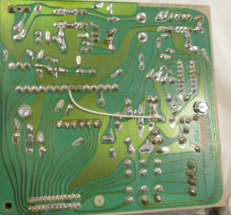
Despite these facts, if you go far enough back, you can find plenty of examples where some artistry made it into a few layers of etched copper. The hand-drawn boards of the 70s and 80s featured swooping curves, contoured splines, and fills only a human could draw. All of these traces served a purpose, but the medium allowed for very organic-looking circuits. In the 80s and 90s, computers were put in charge of drawing traces, and the artistry of PCB design quickly devolved into an easily identifiable pattern: the top layer is horizontal, the bottom layer is vertical, all angles are at forty-five degrees.
In the last few years, the homebrewer has had access to the same tools as the professionals, and with that comes an exploration of materials and techniques. There is a lot to consider. The substrate for a PCB can be fiberglass, teflon, cardboard, and even ceramic. The depth of soldermask and silkscreen color is second only to the depth of your wallet. Even the finishes can be a beautiful matte gold or a shiny reflective silver.
Star did lend a few tips to everyone in the audience. If you’re dipping your toes into the world of artistic boards, Eagle is a great choice. Not only does it do curves, there are scripts to take care of areas of negative silkscreen, and you can import bitmap and vector files.
Given the success of Star’s Circuit Classics, what tips does she have? Iteration, first of all. She has a desk covered with purple prototypes before moving on to mass production. When she got there, the board house was a little confused over Forrest Mims’ art right next to the circuit. This wasn’t documentation, she explained to the fab, this was art that should be on the PCB. Communication with the board house is paramount.


Interesting video – I bought a couple of boards from moeco.jp.net earlier this year, a company who have taken their many years experience in pcb prototype manufacturing and put a little bit of art into their products.
My personal favorite:
http://machinedesign.com/site-files/machinedesign.com/files/uploads/2016/07/11/Untitled-6.gif
Ah yes, but can it steal food from private events on-campus?
It’s good to see Star moving on to PCBs instead of just breadboards but I would still advise her not to stick one on her tshirt and walk about an airport with it.
nice 2009 meme you got there
well of you want an up to date comment I’m happy to oblige
$40 for a slab of fibreglass which is four times the size it needs to be without optimisation is outrageous.
if you want to understand or teach a circuit you do it on a breadboard where changes can be made, effects can be seen, conclusions drawn.
conversely if you want to learn about pcb fab you lay it out yourself, get it etched (with/by adult supervision) and then solder it.
so what niche in the market is this filling? desk trinkets? things to give kids on an open day so they can pretend to their friends how clever they are?
trying to inject beauty into pcb design is sadly flogging a dead horse. anything that is can be autorouted is autorouted because money. anything strict enough to require handwork won’t be conducive to artistic flourishes.
repair industry is almost dead or cheap Chinese labour with no sense of humor but a beautiful layout is certain to warm the hearts of anyone left to notice.
Who cares? It’s cool. What does the other stuff matter?
amen
thanks John
Even with form following function, and computers doing most of the work, there are some boards e.g. motherboards that are aesthetically pleasing.
What is her problem with small SMD components in the beginning of the talk? Come on, it’s almost 2017, time to get into hand soldering 01005, girl! ;)
And the topic around 24 minutes with via tenting, it’s actually very easy to do in Altium. You just make a new rule for solder mask expansion applyed only to vias (IsVia), and give it a negative value to pull the mask in over the via-pad edge. (If you have different via-sizes, you might have to set up one rule per size). Same as you would do with solder mask defined pads, something more common for BGA footprints where you do have teardrop-shaped pads and still only want a circle as exposed copper to get better soldering joints.
The problem with completely tenting vias over is not really that etchant gets trapped inside that would eat away your via over time, since the boards are washed very well after the last etching and before the mask gets applied. It’s a much bigger problem in later production if air bubbles (maybe even with some water after the previously mentioned washing process) get trapped and heated up to 260°C soldering temperatures in a reflow oven. Your board could start to pop like popcorn, blasting away components or ripping fractures in the via. And if you have to clean your board after soldering, good luck getting all the flux and cleaning solvent out of these randomly half closed via-holes again…
Another nifty trick to get a special look on your board:
Go with multilayer and plugged+capped vias, then make the layout so you directly pull all traces to internal layers directly in the component pads. No traces to be seen on the outermost layers. If you go with at least 6 layer boards, you could even completely hide the internal traces by setting layer 2 and 5 as filled polygons, or if you go with 4 layers, at least use one for a complete fill and the other internal layer for all connections (and don’t forget heat traps on the via-in-pad for hand-soldering/rework if they connect to those fills!).
I agree with her that they should basically support splines in layout tools to make nice looking and “wavy” layouts easyer to draw.
Thanks for the contributions!
As for “What is her problem with small SMD components in the beginning of the talk? Come on, it’s almost 2017, time to get into hand soldering 01005, girl! ;)” — I have done rework at this scale previously (most significantly in 2012-2013 or so?) I just don’t recommend it for beginners. It’s not designed for human beings and wasn’t that fun. I don’t really see any guts/glory in manipulating tiny parts (I didn’t have a microscope. If you do, it’s basically same-same as everything else.) The point of the card is to remind myself of that since it can be easy to forget (if you are designing and expect to do any prototyping/assembly yourself) how big something is in real life when everything is scaled up on the screen.
If i have to do layouts with unfamiliar component footprints, my goto solution is to quickly print out the board at 1:1 scale once the rough placement is done and put that next to the screen, just to get a better feeling of the size of the board and component sizes in real life. The footprint library i’m working with usually has the metric dimensions of the component somewhere in the names. This helps me get a better feeling for the size. A 0402 chip capacitor for normal density would be named CAPC1005N (1.0×0.5mm). (I live in metric world, so the millimeter gives me a better reference size in my head than imperial)
Basically if you stick with the IPC-7351B naming convention, you will get a good idea about the real life size of your footprints just by reading its name. I really hate some of the basic librarys of the open-source/free tools where they just call a footprint “SO-8” or something along that line without adding more details like pitch and span in the fooprint name.
The aesthetics of a board can be used as a measure of the amount of effort poured into the project. I’ve worked with many engineers who treat the design process as more of a miserable chore than a labour of love. More often than not, their PCBs would contain ridiculous errors such as mismatched pad landings to fudged length tuning.
Excellent lecture!
im not en expert here but is emi and signal integrity taken into account in these designs? I know pcb trace layout effects both and I really wouldn’t want to spend for a pretty board just to have a bunch of debugging that ultimately ends up coming from prettiness of said board
Naturally! That is the primary concern of the engineer. My talk does not address those elements, because I take this to be a given.
A note regarding the video editing. I had to back up and pause several times to view the photos. The live audience could see the slides as she describes the techniques but the video viewers cannot. CCC vids handle this by showing the slides fullscreen by default and showing the presenter in the corner when needed (and reversing those when needed)