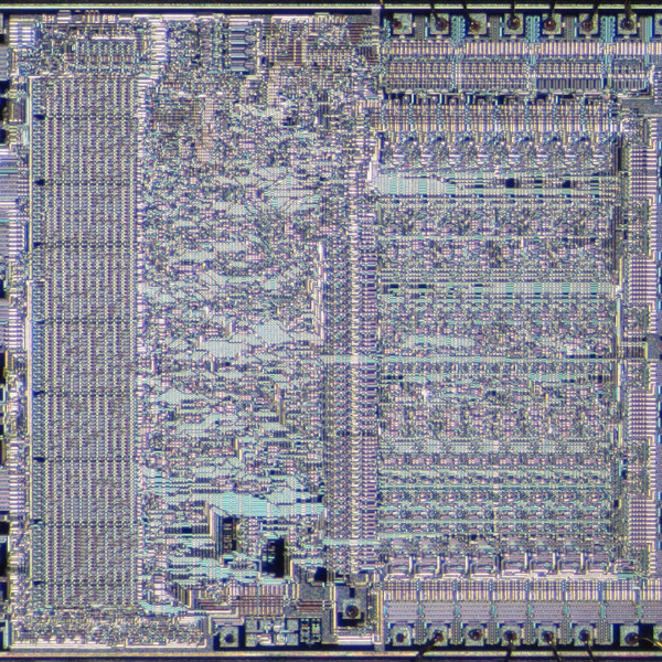
The Intel 8085 microprocessor was introduced 40 years back, and along with its contemporaries — the Z80 and the 6502 — is pretty much a dinosaur in terms of microprocessor history. But that doesn’t stop it from still being included in the syllabus for computer engineering students in many parts of the world. The reason why a 40 year old microprocessor is still covered in computer architecture text books instead of computer history is a bit convoluted. But there’s a whole industry that thrives on the requirements of college laboratories and students requiring “8085 Microprocessor Training Kits”. [TisteAndii] just finished college in Nigeria, where these kits are not locally built and need to be imported, usually costing well over a 100 dollars.
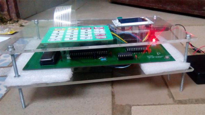
Which is why his final year project was a low cost Intel 8085 Microprocessor Trainer. It’s a minimalist design with some basic read/write memory, program execution and register inspection, with no provision for single stepping or interrupts yet. The monitor program isn’t loaded in an EEPROM. Instead, a PIC18 is used and connected to the 8085 address, data and control pins. This makes it easier to write a monitor program in C instead of assembly. And allows use of a 1.8″ LCD with SPI interface instead of the more usual 7-segment displays used for these kind of kits. [TisteAndii] built a 6×4 keyboard for input, but couldn’t solve debounce issues and finally settled on a 5×4 membrane keypad.
Being a rookie, he ended up with a major flaw in his board layout — he missed connecting the SRAM and the PPI devices to the data bus. A bunch of jumper links seemed to solve the issue, but it wasn’t perfect. This, and a few other problems gave him a lot of grief, but towards the end, it all worked, almost. Most importantly, his BoM cost of about $35 makes it significantly cheaper compared to the commercial units available in Nigeria.
While some hackers may consider this a trivial project, it solves a local problem and we hope the next iteration of the design improves the kit and makes it more accessible.


I’m not at all surprised that half the traces were missing because he is working from a graphical net list instead of a schematic.
What’s being taught today. I see these graphical net lists being called schematics all the time now.
Anyway excellent project. I went to see the “schematic” only to find a graphical net list that gives me no visualisation of the circuit.
And even the layout itself has “slight deficits”. Right angles, very small power traces, unnecessary long traces…. And yes, the schematic would be nicer with busses. 3/10 for the effort.
Ratsnest was pretty daunting for me. Got desperate enough that I used the auto-router for practically all the routing. I’d have probably noticed the omitted chips if I’d done the routing myself. Yes, buses would have been neater. I actually started with them but I decided the effort wasn’t worth it especially when I had more urgent stuff to worry about, like actually getting the thing to work. Of all the things I wish I’d had enough of, time tops the list easily.
Well I, for one, think this is a fantastic effort. I think back to my first PCB layout and it was crap, required many patches, and chips and components were facing every which way. That was when a small PCB would cost a few hundred dollars, 2.5 cents per via, extra charge for solder mask and silkscreen, and take 6 weeks to deliver. I think every electronic or computer student should layout and submit at least one PCB job just for the understanding of the process. I hope you have continued your interest in designing circuits from scratch. (by the way, the naysayers that complain about things like right angle traces are either living in the past or have no idea why decades ago that was an issue but nowadays 45s are for aesthetics only)
All V1.0’s have problems. I cheat and use a lot of programmable logic so that I can fix mistakes that way.
At least the documentation is very good –
https://github.com/brianrho/Rho85/blob/master/docs/Project%20Report.pdf
Well, based on what I was taught that graphical netlist IS a schematic, just a really bad one. I really hate the over use of ports like that, but I can’t argue against the efficiency. 5 minutes to slap those port labels on there, versus 2 hours drawing out all the individual lines.
You don’t draw individual lines. For address and data line you use busses
I wasn’t sure if Eagle had busses.
I use Altium, and I try to avoid busses when I can because of the requirements on net naming, and how they clash with company standards.
Thanks. The graphical netlist you’re referring to is the .sch file, right? I thought I’d uploaded everything relevant; even with a PNG of the schematic. What sort of schematic is expected?
I was referring to schem.png
The question I was really asking is “What sort of schematic is expected now days?”
I am older and I am used to full schematic diagrams that are even useful for repair/servicing. Now it seems that we are in such a “throw away” society that repair is no longer considered.
I used Eagle for the project and I uploaded the .sch and .brd files. I uploaded the PNG so anyone can get an idea of the circuit diagram without needing Eagle. Unless there’s some other file that would provide a more complete description of the schematic? You referring to a SPICE netlist?
What you did (1) vs. what RÖB wanted (2, 3):
https://abload.de/img/unbenannt3csab.png
@SebiR Yeah, I replied earlier about that. I’m a bit confused about his reference to a “graphical netlist” and how it’s different from a schematic. If there’s any additional info I can upload to the repo to make it more complete, then I’d like to do so.
The documentation and the schematic and everything are complete and great. This sort of schematic is just a bit confusing for service. You can’t see at a glance where all the connections go. You have to have the schematic in EAGLE to highlight the connections. When you print it, it becomes quite confusing ;) So, don’t worry, your project and the documentation are great :)
There are a couple of 8085 emulator apps on play.google.com too, if you have an android phone already, and they are free.
Nothing quite beats messing around on real hardware, though.
And the satisfaction when it finally starts doing what it was supposed to do. (Fondly remembering the kits with 80188 on which I learned bare metal programming).
Good old 8085. First chip I programmed on, and still useful for bare metal learning. For a first project, well done (it works :)).
+1
Z80 is better though…
What I don’t really like about the Z80 is the complex timing.
Wasn’t there one of these older CPU’s that had a more modern single-cycle (instructions) clone ???
I am making a Z80 project and I would love to though single-cycle CPU in there and see how it goes.
80C50 – 50C85 or something like that. I think it was microchip.
Huh, so am I my friend!
A few things to keep in mind. Only the CMOS Z80’s (z84c00xx) can be static clocked.
Not the standard NMOS z8400. Also, the z80’s have phenomenal overclocking abilities,
you can push just about all nmos z80’s easily up to 8 Mhz or so.
Yes, that caught me out when I bought some Z80’s from China they were labelled as the higher speed CMOS version numbers but were actually the slower NMOS versions.
PS: you can tell the difference with one of the port instructions.
From memory (google it if you need) the OUT (C), A will place 0xFF on half the address bus on one version and 0x00 on the other – NMOS/CMOS
I found what it was – it’s the (Intel MCS-51) C8051 (FLASH) or C8031(ROMless) that is single cycle in the enhanced version that it available today but it’s Harvard Architecture.
The 8085 is Von Newman Architecture and about 12 clocks to one instruction cycle.
I wish there was a single-cycle 8085
Is it just me or does using a PIC kind of defeat the purpose of a “trainer”? If the purpose is to learn microprocessor architecture than use the 8085 as is, with all of its warts. If the purpose is programming, than just use the PIC.
I found my old 8085 from college electronics, thought I might try to get it working again.
http://i306.photobucket.com/albums/nn275/eugenenine/Misc/IMG_20161002_1615067.jpg
Missing the LCD and ROM and I’ll probably have to start from scratch on new perfboard.
I still have an Intel 8085 trainer, someone moving gave it to me about 1990. But I still have my KIM-1 6502 board from 1979.
About 1978, Byte had an article about bootstrapping the 8085. So you didn’t need rom, you could dingle step it, and by loading the CPU’s data lines with NOP, the CPU would advance through the address range, so you could load the RAM directly. It was all neat and simple.
I later saw a piece about getting the 68000 going the same way. And Don Lancaster’s Cheap TV Typewriter Cookbook counted on the same concept to advance the address bus to be able to get the data out of the RAM for the video.
Michael
“The reason why a 40 year old microprocessor is still covered in computer architecture text books instead of computer history is a bit convoluted.”
Oh come on! That’s how you leave it? You could have said something like “Believe it or not, this 40 year old microprocessor is still the basis of many computer architecture courses.” That would have been just fine. “history is a bit convoluted” that just invites curiosity and leaves us hanging with no satisfaction. I’d say it was an invitation to research the matter ourselves but what search terms would one even use for that?
I’ve seen them in the wild as display drivers for gambling machines and simple things like that.
Indeed, There was a controller board for a commercial laundromat I found that uses it…
I must have gotten rid of my 8085 (and 68k) books a while back as they are not where I expected them to be. So I’m going by memory but IIRC the reason the 8085 is used is its the simplest of the 8080 lineage. The 8080 had more registers and required more support circuitry. The 8088 was more complex to program due to the bank switching. The 8085 can run without any support circuitry and has fewer registers and no bank switching.
As a computer engineering student…I think this is a fantastic project. 60% reduction in price and making learning tools more available for people of less means than me, here in the US? That’s such a fantastic idea!! the flak people are giving him for a less than perfect board design is totally unwarranted–for one student working without pay, what are the expectations? ridiculous how cruel y’all can be, turning projects into a commentary on this false notion of a “participation trophy” generation.
end rant.
FANTASTIC WORK, [TisteAndii].
and old processors are used in architecture classes because they are simple, well documented, and cheap, all valid reasons.
*me in the US, not saying the project is of US origin haha
Thanks :D ! I’m okay with the criticism though; it’s half the reason I had it posted here after all — the uber-community of hardware hackers. Though truth is, most of the mentioned issues are stuff I already knew about but had no time/experience to correct.
First of all, it’s not exactly a trivial project, and it targets a genuine need, so full marks to the project’s creator.
I do wonder why today’s schools don’t make more use of virtualized simple processors and emulators to teach the basic processor architectures, and a hands-on project based onsomething more current like a PIC or AVR, that they’re more likely to encounter in their careers. Kind of a shame to have to cough up $100 (or even just $40) for something that has no practical use (except for bragging rights in HaD) when the course is done. Even an Arduino would get more post-course use.
Because $. Schools don’t understand or even look at pen source, they have been hearing the ‘free is crap’ for so long they think they can only have software thats paid for and those cost a lot of $.
Yup. Or would cry the blues about being out of funding.
Don’t even get me started with the plethora of issues found in the democrap-run school district of Philadelphia.
The external PIC-based monitor is a nifty idea, although I don’t think that writing it in assembly for 8085 is that big of a problem: a very reasonable serial-based monitor with breakpoint support fits in just a bit over 4kb of code and even that’s a bit much – the code can be squeezed further by factoring out more subroutines. It certainly is more of a challenge than writing in C, but a “raw” 8085 is much easier to bootstrap without special tools than a PIC. I somewhat dislike proprietary programming tools and think that such a low-cost project could target the bare minimum.
Here’s an alternative to how it could be done: low-cost FTDI USB interface chips support a parallel mode where the pins are essentially GPIO. This can be used, with very minimal glue logic, to load RAM with code. The code in RAM would boot to a copier that programs the EEPROM with the monitor code (of course included in the RAM). A jumper could then be used to switch the RAM and EEPROM mappings, so that the device would boot from EEPROM after such bootstrap. For minimal cost, EEPROM can be left unpopulated, so that the board would need to be loaded with firmware via USB on every power-up – not a big deal if cost is truly the driving factor.
Even though 8085 may be considered “completely” obsolete, it still is a wonderful target to teach the basics of microcomputer architecture. Even with peripherals the entire development board can be completely documented in less than 100 pages, and that includes instruction set, architectural description, registers, whatever peripherals are present, etc. Once you read it, you know everything there is to know about the hardware: nothing is hidden.
In contrast, complete documentation for a Raspberry Pi is about 15,000 pages and some of it requires signing a non-disclosure agreements with Broadcom, and some of it is of rather poor quality or has mistakes that take lots of time to figure out. So using the Pi as an architecture teaching tool for novices is an absurd proposition, yet somehow it sometimes is used just for that purpose. On the Pi, the ARM cores are secondary, and you can learn a smaller and easier to comprehend subset of architecture by leaving the ARM out. The tool support is abysmal though, and those NDAs make it virtually impossible to use in teaching.
And documentation wise, the Intel manuals serve as a decent example of how to write engineering documentation for microprocessors. It is apparent that some people who document modern chips have never had that experience… :(
So, I’d say that India is doing something right here. Using a simpler architecture to teach the basics has solid pedagogical grounds, and also provides the students with confidence, whereas working with modern microcontrollers can feel like black magic – there are documentation bugs, there can be thousands of pages of a manual to deal with, the runtime libraries for the C environment are a black box, and so on.
Myself – I started to learn this on Z80 back in the early 1980s, and I think it has instilled in me some sense of what it means to truly understand an architecture. Given the complexity of modern SoCs, such total understanding is essentially impossible.
I hasten to add that the total understanding doesn’t need to be a goal in itself, but can be used as a reference to judge one’s own understanding of more complex systems. Even an AVR Arduino UNO is not a target that student can be expected to master in less than a couple of semesters, because of how complex the tooling is – and to truly understand it you basically have to start by writing a minimal C runtime, learn the gnu toolchain including the linker scripts, and so on. 8085 can be reasonably programmed with a linker-free assembler, and those run straight in the browser these days, with direct .hex and .bin output – it doesn’t get any simpler than that. Sure – learning the gnu toolchain on a “simple” target like an AVR is not a bad idea, but it does add layers of abstraction that can get fairly confusing for students without prior experience. It took me long enough as a kid to figure out how to use the comparatively simple 8080 toolchain on CP/M (assembler, linker, relocator, dumper) – and I had some parental support in that, and almost unlimited time.