We are used to stories about reverse engineering integrated circuits, in these pages. Some fascinating exposés of classic chips have been produced by people such as the ever-hard-working [Ken Shirriff].
You might think that this practice would be something new, confined only to those interested in the workings of now-obsolete silicon. But the secrets of these chips were closely guarded commercial intelligence back in the day, and there was a small industry of experts whose living came from unlocking them.

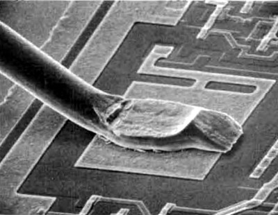
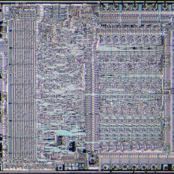
Integrated Circuit Engineering Corporation were a Scottsdale, Arizona based company who specialised in semiconductor industry data. They have long since been swallowed up in a series of corporate takeovers, but we have a fascinating window into their activities because their archive is preserved by the Smithsonian Institution. They reverse engineered integrated circuits to produce reports containing detailed information about their mechanical properties as well as their operation, and just such a report is our subject today. Their 1979 examination of the Zilog Z80 CTC (PDF) starts with an examination of the package, in this case the more expensive ceramic variant, then looks in detail at the internal construction of the die itself, and its bonding wires. We are then taken in its typewritten pages through an extensive analysis of the circuitry on the die, with gate-level circuits to explain the operation of each part.
The detail contained in this report is extraordinary, it is clear that a huge amount of work went into its production and it would have been of huge value to certain of Zilog’s customers and competitors. At the time this would have been extremely commercially sensitive information, even if it now seems like a historical curiosity.
The Z80 CTC is a 4-channel counter/timer peripheral chip for the wildly succesful Z80 8-bit microprocessor, in a 28-pin dual-in-line package. We were surprised to find from a quick search that you can still buy this chip from some of the usual suppliers rather than the surplus houses, so it may even still be in production.
If IC reverse engineering takes your fancy, take a look at our archive of [Ken Shirriff] posts.
Thanks [fortytwo] for the tip.


You are forgetting one of the big motivators for pouring a lot of resources into ROing silicon. Patent infringement.
There’s a whole ecosystem out there, including offensive patents such as patents on how to camouflage silicone reverse engineering efforts. Like US patent 6979606 for example.
That and lawsuits. I worked doing this sort of thing for a “big semiconductor manufacturers” in the mid 1980s. The tools of the trade included heavy optical microscopy tables. X-ray, SEM, Auger, EDS/XDS, and SIMS. We had equipment to lap cross sections, and fabricate really tiny needle points to use as probes.
Most of what we did was troubleshoot yield problems. Sometimes we would analyze customer issues. Sometimes you did analysis on competitor’s parts to look for patent infringement or things you could report out about their technology. And sometimes you got a CPU out of a car that had killed someone. There was a lawsuit. And the accusation was “the car’s computer failed”. Those were tough because they were singular pieces of evidence in a case so they had to be handled certain ways.
We all had different specialties. I was never very handy dropping probes down on the die (I could do it, but had more mess ups then most). But I was good at diagnosing problems (we should look here). And building test setups for exotic conditions. One guy was really up on the process issues. We had one guy who had done it for years and he was patient enough to just look for odd things and find them (tough because if the die were the size of a football field, you would be looking at it maybe a square inch or less at a time in the microscope eyepiece). It was a good team, but bad management drove me out of it. Other than that it was probably the most fun job I ever had.
Wow. That’s really cool!
Wonder how well they would have done with something as complex as today’s microprocessors?
SEMs, saws to cut cross sections, lapping, x-ray, probing for destructive analysis.
For non destructive testing, LIF (laser induced fault) probing, IR imaging (both for hotspots and light emitted by junctions), JTAG scan dump / BIST / boundary scan, and lot traceability.
You may be surprised that it is still being done by ICL in Tempe, AZ. And mind this is an OLD report. During my time (2000) ICE did latest microprocessors like the IBM Power PC series.
Speaking as the manager of the laboratory at integrated circuit engineering, corp. we would have used the same or similar analytical techniques, adding fib and tem cross sectioning to supplement the manual cross section polishing. we were constantly evolving our analytical techniques to keep up with the always-changing semiconductor technology changes. we performed physical construction analysis for competetive analysis and patent support, and also physical failure analysis. My team of laboratory analysts, was the best in the industry. i am retired now, but happy to answer any questions, my email is chippatents@gmail.com.
That is fascinating!
really love this, its a piece of history and also a work of art. Z80 was the heart of the ZX spectrum, RESTECP!
Did you notice yourself becoming entranced by the ICE report? Could it have been because it’s been so long–if at all–since you’ve seen a type-written report? And remember: if the typist made a mistake, the entire page had to be re-typed (at least in high-quality organizations, and most certainly for formal reports). Almost a work of art, examples of which are not seen any more. Certainly a work of hard work and expertise.
Enjoyed reading your story and reliving my past! I worked in (from 1979 to 2003) and managed the laboratory services group that performed the analysis and created those RE reports (might actually have taken those pictures).Those were the good old days!!