The Art Of The Silicon Chip

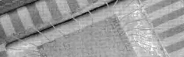
If you have followed the group of reverse engineers whose work on classic pieces of silicon we feature regularly here at Hackaday, you may well be familiar with the appearance of the various components that make up their gates and other functions. What you may not be familiar with, however, are the features that can occasionally be found which have no function other than the private amusement of the chip designers themselves. Alongside the transistors, resistors, and interconnects, there are sometimes little pieces of artwork inserted into unused spaces on the die, visible only to those fortunate enough to own a powerful microscope.

Fortunately those of us without such an instrument can also take a look at these works, thanks to the Smithsonian Institution, who have brought together a gallery of them on the web as part of their chip collection. In it we find cartoon characters such as Dilbert, favourites from children’s books such as Waldo, and the Japanese monster Godzilla. There are animals, cows, a leopard, a camel, and a porpoise, and of course company logos aplenty.

In a sense, these minuscule artworks are what our more strident commenters might describe as Not A Hack, but to dismiss them in such a manner would be to miss their point. Even in an age of huge teams of integrated circuit designers working with computerized tools rather than the lone geniuses of old with their hand drafting, we can still see little flashes of individuality with no practical or commercial purpose and with no audience except a very few. And we like that.

Also take a look at the work of [Ken Shirriff] for a masterclass in IC reverse engineering.

Integrated Circuit Reverse Engineering, 1970s Style

We are used to stories about reverse engineering integrated circuits, in these pages. Some fascinating exposés of classic chips have been produced by people such as the ever-hard-working [Ken Shirriff].

You might think that this practice would be something new, confined only to those interested in the workings of now-obsolete silicon. But the secrets of these chips were closely guarded commercial intelligence back in the day, and there was a small industry of experts whose living came from unlocking them.

Electron micrograph of a wire bond to the Z80 CTC die

Integrated Circuit Engineering Corporation were a Scottsdale, Arizona based company who specialised in semiconductor industry data. They have long since been swallowed up in a series of corporate takeovers, but we have a fascinating window into their activities because their archive is preserved by the Smithsonian Institution. They reverse engineered integrated circuits to produce reports containing detailed information about their mechanical properties as well as their operation, and just such a report is our subject today. Their 1979 examination of the Zilog Z80 CTC (PDF) starts with an examination of the package, in this case the more expensive ceramic variant, then looks in detail at the internal construction of the die itself, and its bonding wires. We are then taken in its typewritten pages through an extensive analysis of the circuitry on the die, with gate-level circuits to explain the operation of each part.

The detail contained in this report is extraordinary, it is clear that a huge amount of work went into its production and it would have been of huge value to certain of Zilog’s customers and competitors. At the time this would have been extremely commercially sensitive information, even if it now seems like a historical curiosity.

The Z80 CTC is a 4-channel counter/timer peripheral chip for the wildly succesful Z80 8-bit microprocessor, in a 28-pin dual-in-line package. We were surprised to find from a quick search that you can still buy this chip from some of the usual suppliers rather than the surplus houses, so it may even still be in production.

If IC reverse engineering takes your fancy, take a look at our archive of [Ken Shirriff] posts.

Thanks [fortytwo] for the tip.

Rebuilding A Custom IC Saves HP Pulse Generator


Rebuilding an HP Custom IC
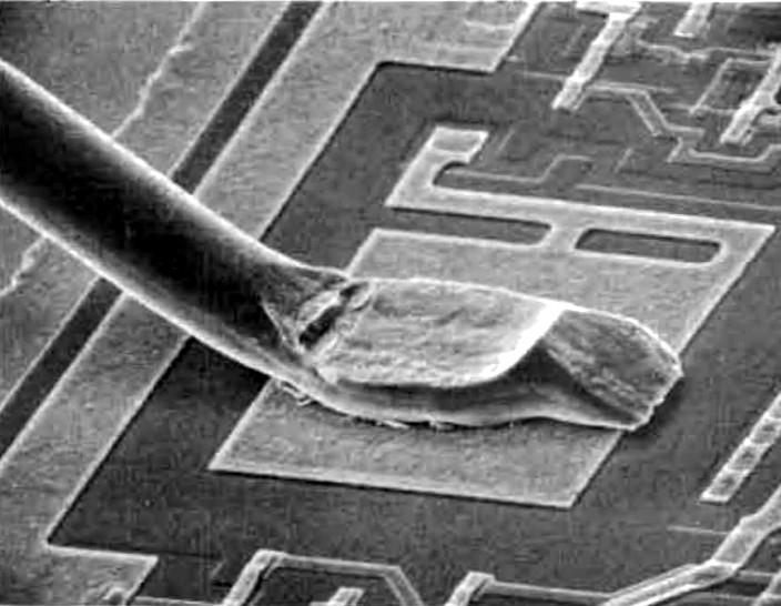
[Matthew] got himself into a real pickle.  It all started when he was troubleshooting a broken Hewlett Packard 8007A pulse generator. While trying to desolder one of the integrated circuits, [Matthew] accidentally cracked it. Unfortunately, the chip was a custom HP Pulse shaper IC – not an easy part to source by any means. That broken chip began a 5 year mission: to explore strange new repair methods. To seek out new life for that HP 8007A. To boldy fix what no one had fixed before.

[Matthew’s] first repair attempt was to build a drop in replacement for the HP chip. He took a look at the block diagram, and realized the chip was just some simple logic gates. He built his version with a small PCB and Fairchild TinyLogic gates. Unfortunately, the TinyLogic series is fast CMOS, while HP’s original chip used Emitter-coupled Logic (ECL). Thanks to the wildly different voltage levels of the two logic families, this design had no chance of working.

Five years later, [Matthew] was going to school at MIT, and had access to a wire bonding machine. He rebuilt the package using some epoxy, and managed to re-run the various bond wires. While everything looked promising, this attempt was also a failure. After all that work, the chip was blown.

Continue reading “Rebuilding A Custom IC Saves HP Pulse Generator”