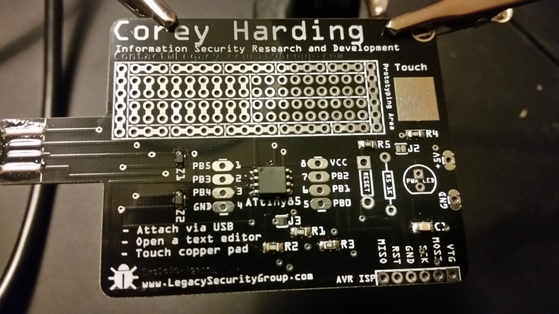
[Corey Harding] designed his business card as a USB-connectable demonstration of his skill. If potential manager inserts the card in a USB drive, open a text editor, then touches the copper pad on the PCB, [Corey]’s contact info pops up in the text box.
In addition to working as a business card, the PCB also works as a Tiny 85 development board, with a prototyping area for adding sensors and other components, and with additional capabilities broken out: you can add an LED, and there’s also room for a 1K resistor, a reset button, or break out the USB’s 5V for other uses. There’s an AVR ISP breakout for reflashing the chip.
Coolly, [Corey] intended for the card to be an Open Source resource for other people to make their own cards, and he’s providing the Fritzing files for the PCB. Fritzing is a great program for beginning and experienced hardware hackers to lay out quick and dirty circuits, make wiring diagrams, and even export PCB designs for fabrication. You can download [Corey]’s files from his GitHub repository.
For another business card project check out this full color business card we published last month.


Cool project. I guess it plays a keyboard and types the contact information (hopefully) into the just opened editor?
And… Fritzing is Free Software. Yay!
i thought one of the HaD commenter mantras is “Friends don’t let friends Fritz”.
Hopefully there is enough room to put some spyware on the card, and find out how you stand in the interview process, or
corrupt other resume’s on his PC…
B^)
You can certainly convert a “Ducky Script” payload to run on this and it looks like you can program the application over USB as a Digispark using the Arduino IDE.
So find or write a ducky script payload then go to:
https://nixu-corp.github.io/
Select digispark under board.
And done!
> Information Security
“If you *actually* plugged this into your machine, you definitely need us”
Just what I was thinking…
I would think that an Information Security guy would be trying to prevent employees from plugging in random usb devices.
Cool implementation though.
Just what I was thinking…
Yeah, if someone were to hand me something like that, I would say thanks and put it aside, never intending to plug it in. If they persisted, I would hand it back to them and state “sorry, no offense, but, I do not plug in unknown devices into my computer”.
Not only does one have to worry about spyware, also, what if it were damaged, say, shorted? or draw too much current?Not sure how a typical USB port handles those circumstances.
Anyway, It’s great little thing to show off ones capabilities, but not original, and probably not going to make them stand out in any way.
Hm. Hey, this gives me a (bad) idea.
Step 1: Print business cards with fake info or for someone you don’t like.
Step 2: Add a ‘USB killer’ circuit (5->100sV boost converter charges a few bigass capacitors that discharge with reverse polarity once they’re charged, repeat until 5V isn’t being delivered anymore.)
Step 3: Scatter around conference.
If I received one of these I would get very curious. Old, PCs are plentiful. Why not dig one out of a closet and see if it catches fire, does something amazing or falls somewhere in the middle. Just don’t plug in the network jack!
That PCB job is just plain horrible. Right angle routing, vias everywhere on such simple board, “autorouter” screaming from all over the board, solder plated USB pins saying “plug me in to make your gold plated contacts lead plated”, confusing mix of SMD and through-hole …
No offense to anyone, my boards from not so long ago looked much much worse than this, but it’s not a good idea to offer job like this to someone as a “proof of skill”.
Well, if we are going to make changes to the design, since it is open source.
I don’t think it is possible to use any standard DIP package in the prototyping area (unless you wire the chip from the under side of the board).
Also, downloading some ones open source design, slapping your name on it, and then passing it off as your “proof of skill”, seems a bit shady. ;)
Right angle routing is not that bad actually. Please read this : http://ieeexplore.ieee.org/document/801409/
However I do agree on the fact that this is a bad advertisement for his skills.
None of that really bothers me. Even the solder blobbed contacts, since even SparkFun does that to make PCB edge USB-A connections work.
I do take issue with the flux all over the USB connector. Security problems aside, I wouldn’t plug that thing in any PC I care about.
Thanks for the constructive criticism. The SMD components are the only components that are required for it to function and so it can maintain a reasonable thickness to fit into a wallet. The through hole components are for the recipient of the card to play with, assuming most people are intimidated by SMD and might actually tackle soldering a through hole component. As far as right angles, you got me there, but auto-router didn’t do it, I have actually never seen auto router work well, I knew someone would say something about the bends though eventually, but I’ve heard that to be both a myth and inapplicable to frequencies under 1GHz, but I am not an expert there I just know 45 degrees is the standard. I could certainly clean it up and save space with different degree angles and routing more of a trace on the top or the bottom, and a ground fill was not used because I have heard of issues when combined with with capacitive touch sensors, coils, etc, and didn’t try otherwise, this may also be a myth though but I assume it to be a terrible idea to place a ground fill on the opposite side of the board directly under a capacitive touch sensor. On to the vias… well maybe they are constellations and its also a star finder? Not really, I actually didn’t realize how carried away I got there until you pointed it out. Its just an open source project for people to have fun with and even you guys had fun in the comments. But it does function as intended. And the prototyping area is more for simple stuff like the user adding and LED to blink or something like that but a DIP package will work as you said by wiring from underside of the board, DIP package occupying the outside and jumpers ran from the inside. Also the board pictured has not been cleaned yet, I imagine someone mentioning this as well. It actually started off a lot simpler than it is now, maybe that was better. I will keep all of this in mind and it is basically just a prototype and I plan on revisiting this project later. PS: To the other comments it could also certainly be used to perform a keystroke injection attack.
Breathe.
Don’t worry, effort is clearly visible, just needs some polishing before using it as proof of skill.
If it’s a capacitive sensor, though why take the mask off? There is usually the mask over them, at least the ones I have seen.