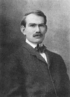
Bill Shockley brought the transistor to a pasture in Palo Alto, but he didn’t land there by chance. There was already a plot afoot which had nothing to do with silicon, and it had already been a happening place for some time by then.
Often overshadowed by Edison and Menlo Park or Western Electric and its Bell Labs, people forget that the practical beginning of modern radio and telecommunications began unsuspectingly in the Bay Area on the shoestring-budgeted work benches of Lee de Forest at Federal Telegraph.
As the first decade of the 20th century passed, Lee de Forest was already a controversial figure. He had founded a company in New York to develop his early vacuum tubes as detectors for radio, but he was not very good at business. Some of the officers of the company decided that progress was not being made fast enough and drained the company of assets while de Forest was away. This led to years of legal troubles and the arrest of many involved due to fraud and loss of investors’ money.
De Forest, who thought that the only problems in his way were technical and could be solved in time, made his case to Federal Telegraph. In very short order his early patents were licensed to others including Bell Labs who quickly developed them into the first telephone relay tubes.
Federal Telegraph was interested in the development of Continuous Wave (CW) radio as opposed to the then more common spark type transmitters. The technology was developed by Valdemar Poulsen in Holland, and used an arc converter transmitter to produce a stable sine wave that was more efficient and less noisy reducing interference with other stations. With this in mind, Federal and de Forest realized that de Forest’s tube could be used for linear amplification and could be applied to it for modulation of speech transmission.
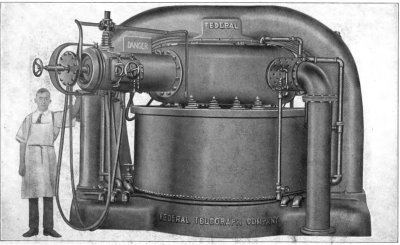
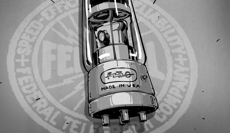
Most of de Forest’s enforceable patents expired in 1925, and an arms race took off with companies such as RCA, GE, Sylvania, and Westinghouse. At that time these companies were aggressively pursuing, mainly through patent litigation, new companies developing better tube technology.
To get the real story you must follow three very important people who worked at Federal and their subsidiary, the Heintz and Kaufman tube company. Charles Litton, William Eitel, and Jack McCullough were all amateur radio operators and understood the limitations of the currently available tubes being offered by large eastern firms.
Litton in particular spent much time devising machinery and new practices at Federal Telegraph’s Heinz and Kaufman tube division that not only side-stepped other patents, but got him many of his own. Soon, Federal was making better more reliable tubes capable of higher efficiency and frequencies than the large makers. Unfortunately Federal Telegraph was acquired by ITT. In their race to consolidate companies they slashed Federal’s budget and moved operations to New Jersey before the new tube designs could attain market success. This led to a technology gap between what was available and what these men knew could be done. Necessity being the mother of invention, these three founded companies to produce these designs and kick off modern radio communications electronics.
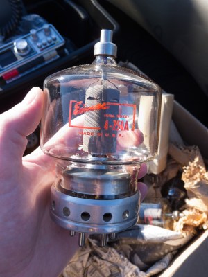
Unwilling to move with Federal to New Jersey, William Eitel and Jack McCullough founded Eitel-McCullough (later shortened to Eimac) to continue producing new and better power tubes, selling them directly to hams and engineers alike. At the same time, Charles Litton founded Litton Engineering to design and manufacture laboratory grade tube assembly equipment for any company wishing to enter the business. His glass lathes are still to this day the standard in the laboratory glass working industry. Together these two companies laid down the fertile soil from which precision high power designs could grow.
Enter Frederick E. Terman
A New Arrangement Between Business and Academia
Widely regarded as the father of what we consider electronics today, Frederick E. Terman’s 1955 fourth edition of Electronic and Radio Engineering still stands as the best textbook on classical electronics and radio engineering. Terman attended graduate school at MIT and saw how eastern business and education operated. He thought that if true advancements were to be made a new attitude toward commercialization of research discoveries was needed.
Terman returned to Stanford as a member of the faculty and his first order of business was to hire Charles Litton and Carl Spangenberg to help him found his Vacuum Tube Laboratory. Spangenberg later went on to become a tube industry expert and writer of the book simply titled Vacuum Tubes. The result of these first hires was a lab dedicated to educating students in not only electronics, but the manufacturing methods needed to push the field forward — a very novel approach in those days. In 1938, Charles Litton gave a $1,000 grant to the lab to hire Terman’s favorite student David Packard on and Bill Hewlett was brought in by Karl Spangenburg. Charles Litton served as a mentor to Bill and Dave in the founding of Hewlett Packard in 1938.
From Radios to Radar
Tube technology in the valley didn’t constrain itself to radio communications. An important invention from brothers Russel and Sigurd Varian affected radar research throughout the world. The British were already using radar system, but the weight of those designs prevented radar from being deployed in aircraft. The Varian’s invention of the klystron solved the weight problem.
Russel and Sigurd Varian were born in California. Russel attended undergraduate school at Stanford, worked in the oil industry earning him his first patent for a vibrating magnetometer, and later worked under the great Philo Farnsworth. Sigurd was not very successful academically, and left college to work a number of different jobs. He found his way into the aviation industry as both a pilot and mechanic. While flying, he would envision the need for an electronic navigation and warning system to allow safe travel at night, in bad weather, and likewise identify the location of a plane in flight from the ground for defensive systems. Russel suggested this could be accomplished with microwave signals. With an eye towards the unavoidable war with Germany they set about to create their system. They failed, at first.
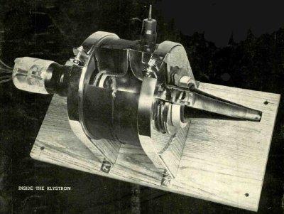
Enter their friend William Webster Hansen. At this time William was a professor at Stanford and on his recommendation the physics laboratory (and not the tube research lab) decided to hire the brothers to develop their system in exchange for lab space and a small budget with the understanding that half of any royalties earned from their discoveries would be shared with the university.
With this backing they developed their own method of velocity modulation in 1937. Velocity modulation had already been demonstrated by A. Arsenjewa Heil and Oskar Heil in 1935, but not published anywhere the Stanford team would have found it. Russel designed, and Sigurd figured out how to build the first klystron, the first practical mobile microwave device. The brothers, Hansen, and Edward Ginzton founded Varian Associates. Now called CPI for Communications and Power Industries they continue to produce power tubes, klystrons, and magnetrons and now own Eimac as well. They also were instrumental in creating radio therapy and radiation treatments for medical use in oncology.
Valley Talent Recruited for War Effort
The war effort put intense focus on the development or radio technology. All of these scientists were hired by New England firms and universities to work on radar systems. Much of it was never made public, but many advances made in tube manufacturing techniques were made during this time. In particular, Charles Litton was the one who made microwave tube manufacturing possible using new tube manufacturing methods he had pioneered.
After the war all of these men returned to their businesses in California. Eitel-Mcullough, Litton Engineering, and the Varian Brothers, Bill and Dave, and the Stanford professors were well versed in selling tubes to the military and what the road map ahead of microwave design would be. Whole new areas of high frequency design and experimentation were now unfolding at a rapid pace, enabled by the research done on the radar projects and the now available war tested high power microwave products now available and Stanford wanted to be the place business went to to commercialize these new technologies.
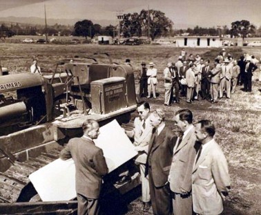
Fredrick Terman realized that they needed to entice companies into investing with Stanford. Proximity seemed to be a good place to start. The decision was made to set aside some university land, most of which was either marsh or farm land at the time, to develop into the worlds first industrial park. Varian Associates were the first tenants, followed by HP, GE, and a number of aerospace firms such as Lockheed. The businesses got cutting edge research and the university got industry-leading guidance and assistance, and most importantly funding. This partnership is really what started technology in the Santa Clara Valley, not transistors.
Goodbye Glass Tubes, Hello Semiconductors
Nobody would deny that the solid state transistor would change the world. In microwave the smaller you can make a device the more efficient it will be, and these companies understood that. They also understood they needed to be at the forefront.
William Shockley, having grown up in Palo Alto, needed a place to set up shop. He had burned his bridges at Bell Labs, and some of his colleagues there felt he did not deserve his acclaim as inventor of the transistor. Stanford was now producing world class engineers fully up to speed in the newest technologies. The Valley was the logical place for him to go.
William Shockley. Evidently nobody liked him, but that’s another story.
Sources for this Article:
You should read The Secret History of Silicon Valley by Steve Blank. Its an excellent book that covers many topics not touched on in other typical Silicon Valley books. Much of the information in this article was sourced there, but is backed up with the countless conversations I was blessed to have with retired engineers in my personal research into the history of vacuum tubes and technology. I would like to thank them all, but many of them are unfortunately no longer with us.
I would like to thank in particular Mr. Howard M. Brady who passed away several years ago. He worked for Federal Telegraph during their New Jersey years and also with Chatham, United Electronics, and Electron Technologies Inc where he was still making strides in research in high vacuum measurement technology right up until the end. When the world was in trouble, he was one of the “experts” who was called to consult with when the answers couldn’t be found in any textbook. Many of the devices and techniques he developed as far back as the late 50’s are still considered trade and security secrets. Over the course of many pleasant conversations he gave me directions to research to put together the story of why things are the way they are in electronics and on who’s shoulders we really stand.





” At that time these companies were aggressively pursuing, mainly through patent litigation,…”
Sound like today…
On PBS’s “Empire of the Air” Lee de Forest was depicted in a less than desirable light. Most notably, his inability to defend his patents against Armstrong in court. He may have won the lawsuit (I don’t remember) but could not explain how his patented vacuum tube circuits worked.
A cow-orker at the place told me of seeing klystrons that were about 4 feet tall and 3 feet wide at another radar facility.
Klystrons started small and were mostly used in WWII aircraft radar receivers, the British invention, the cavity magnetron had the high power pulse capability that made aircraft radar transmitters possible and the whole radar system worked because of a Dutch developed pentode valve technology smuggled out of Holland after the German invasion of Europe.
Later klystrons for radar and TV transmittersetc got very big as you described.
If you’re in the Bay Area and want to see some decent sized klystrons, see if you can wangle a tour at SLAC, they have ~3 km of them on top of the beamline.
Yes, what I recall from reading was that De Forest could only see the tube as an amplifier. Armstrong in coming up with regeneration for receiving also showed how to use tube for generating a signal. De Forest pounced, and I think he won some of the claim, but no, he couldn’t explain it.
Howard Armstrong is amazing, getting a patent for the regenerative receiver, the superheterodyne receiver, and the superenerative receiver. Those three account for just about any receiver beyond the very early “crystal” and TRF receivers. The superegenerative wasn’t too practical at lower frequencies so they were never mainstream, but they helped moved into the higher frequencies, and in endless license free walkie talkies, and I gather still seeing some use in some remote control things like garage door openers. Even software defined radios still often count on heterodyning signals own to a lower frequency for processing, so are descendants of the suoerhet. Then Armstrong went on to show the value of wideband FM. That’s one person. Yes, if held not done all that likely others would have come up with them, but he did it by himself. It’s not just the foundation of radio, but electronics in general, since everything uses electronic oscillators.
And Armstrong had to spend a lot of time defending those patents, he kept getting challenged.
Michael
Reminds me of a funny story. Sadly I don’t remember all of it. But a friend of my Dad’s was in an Army unit with Armstrong. He and some friend’s thought this was an outrageous waste of talent, so against Armstrong’s wishes they got in a phone booth and made a call to someone one of them knew. The upshot was Armstrong was transferred to a proper technical job.
From my experience in Software Defined Radios the easiest and cheapest way to process them is grabbing an audio chip and heterodyning them down to audio freqs. The last SDR I worked on used a Blackfin processor, then it was all DSP from there.
For the first time a regenerative receiver circuit can be recorded in the works of Tesla, as probably many other fundamental schema in EE aria. One can look at his Colorado Spring Notes 1899-1900 (14 years before the Armstrong first patent), at page 136-137, with title of “Self-exciting process”, where Tesla shows different type of, spark gap based, regenerative receivers and correctly identifies that this technique for signal magnification will have quite many valuable uses in the future.
This information is not to diminish the work of Armstrong, but to show that such circuits were invented as tools, in the standard process of their work, by some of the great inventors such as Tesla, as part of their practical tool set, and these circuits were used as tools to create particular engineering artifacts they were working on.
This link doesn’t works: “Electronic and Radio Engineering”
It appears to have broken. You can find it on Amazon
https://www.amazon.com/Electronic-Radio-Engineering-Electrical/dp/0070635099
I will try to find a better link to it.
This book is freely downloadable from:
https://archive.org/details/RadioEngineering
scroll down to see the available downloable formats.
Thanks, I almost bought one of the the books until I saw your link. I love working on old vacuum tube radios and we can never have too much information!
Note that vacuum tubes are still in common uses. Magnetrons used in every microwave oven is one. Traveling wave tubes used in satellites communication are too.
from wikipedia: “TWTs account for over 50% of the sales volume of all microwave vacuum tubes.[1] They are widely used as the power amplifiers and oscillators in radar systems, communication satellite and spacecraft transmitters, and electronic warfare systems”
I used to work on a radar that used TWTs with 13 amp helix current, 37,000 volt cathode plate difference, and about 4 meters long.
I think this is a great article.
Thanks!
William Shockley started the semiconductor boom in Palo Alto.
But it wasn’t the existing industry that drew him there. His mother lived there, and she had become seriously ill, so William moved out there to take care of her.
Shockley semiconductor and the many companies that spun off from it had little to do with the local industry. They were making fantastic new devices for the world.
If you think about it, there’s more silicon in a vacuum tube than an IC…
But it is in amorphous form and one can see through.
I see through your thinly veiled disparagement of vacuum tubes!
B^)
Not only in the glass but the Mica is nearly half silica.
“Many of the devices and techniques he developed as far back as the late 50’s are still considered trade and security secrets.”
That in itself would be worth an article.
If anyone could write it.
I don’t even begin to know who to ask to get permission to talk about that stuff! The things covered in his patents of course are public. Many of his patents were about extending the range of iron gauges below the x ray effect threshold. Not sure I can make anything worth reading out of that.
John Fleming invented the vacuum tube diode, the first useful thermionic device. This was used in early radio before de Forest’s triode.
Correct. De Forest was actually trying to make a more sensitive detector at first.
In fact, the Fleming valve was never anything more than a direct copy of the Edison Effect diode, with which he was very familiar. Many years later he had the bright idea of using it as a detector of radio waves. I do not understand how he could get a patent for a diode which was well known in the literature. In 1943, when Marconi sued the U.S. government, the U.S. Supreme Court held the Fleming patent to be invalid.
Ehh… Poulsen was Danish, not Dutch.
Oops. My mistake.
@Charles Alexanian, As an EE that regularly designs with high power TWTA and Klystron power amplifiers, this is a nice introductory article regarding the evolution of these devices. You did very well with this one Charles. Thank You…
Thank you. I was having a really hard time trimming it all down to something radially read. There is so much that happened during those days that I was having real trouble with it. Fortunately there are some excellent books about that time people can read for an in depth story.
History is something missing from the internet. The hobby electronic magazines would often articles dealing with electronic history, though not too deep and lacking references. But I did get a lot of history that way.
But on the internet, few take the time to write about history. But how things develop is interesting. An idea doesn’t come out of nowhere.
I had a great book out of the library fifteen years ago, something like “The Invention that Changed the World”, about Radar development during WWII. Things had advanced, but the need for radar caused lot of development of electronics, including pushing the use of ever higher frequencies. And while they could create transmitting tubes, receiving was a problem, until they went with cats whisker’s, then to a more stable device. The book made the case that those microwave diodes were the foundation of semiconductor diodes and transistors after the war.
And without radar, there’d be no “radar ovens”, ie microwave ovens.
Michael
Glad someone invented chocolate too. ;-)
Great article and really well put together. Awesome references as I’ve not read into Philo Farnsworth so much until now. Vacuum systems make sense. I sometimes wonder if the IC’s and other solid state materials that won’t sublime can be placed in a vacuum tube to improved performance. That along with cryocooling which the gentleman jacques1956 reminded me of with satellites. In space they have the shade advantage I assume for the electronic devices if they’re super-insulated well to keep the other hot side heat out. Seems superconducting and vacuum’s go together well. Now, heat exchangers coupled with the devices/components in a vacuum tube seems like a way to go moving ahead. MEMS cryocoolers maybe? Peltier Effect doesn’t seem efficient yet unless they haven’t approached a theoretical size limit in their device manufacturing. I don’t understand that effect well enough yet.
Actually the internal temp of a Hughes spinning satellite in orbit was about room temp.
It depends on several factors. Spinning satellites tend to average out. Non spinning ones depend on the emisivity of the surfaces and which way they happen to be pointing.
Makes sense also with more consideration to materials properties of the internal systems, boundaries and environmental conditions. Thanks again and really great article.
Makes sense. Thanks for sharing.
Makes sense, for their distance from the Sun.
Maybe it should be called Silica Valley then.
Story with a gritty feel to it.
I really enjoyed this article. Full of interesting stuff I only knew small parts of, and very well written.
In my first career, I was occasionally handling the big power tubes from Varian and Eimac (broadcast transmitters), but I didn’t know anything about the companies.
Well done!
Philo Farnsworth…perhaps the best name ever. Although it sounds more appropriate for a barnstorming pilot.
A couple of books I enjoyed about the beginnings of radio:
Syntony and Spark:
https://muse.jhu.edu/book/34260
The Continuous Wave:
https://muse.jhu.edu/book/33609
The most recent issue of Nuts and Volts had a vacuum tube article, also. Happy to see them treated as something other than esoteric devices, discussed in passing on the way to transistors.
I had a summer job throughout high school as an electronic repair technician, after completing a correspondence course in electronics that eventually resulted in getting a First Class Commercial FCC license. One of the first devices the business had me repairing were Litton commercial microwave ovens used in the local restaurants. I wasn’t familiar with the founder previously, so enjoyed reading about him here.
Electron Tubes make semiconductor manufacturing possible. Today these tubes are made using stainless steel rather than glass but still consist of an electron gun generating an electron beam inside the evacuated tube controlled by electric or magnetic fields . All semiconductor masks are made using electron and ion beams. Wafer inspection is done using the electron microscope which is an electron beam that scans the wafer. Since the electron has a wavelength of about 1nm, compared to hundreds of nm for photons (light), they can be used to make a semiconductor at much smaller geometry than using light. However, the throughput is much slower than using lithography which is why the semi industry is spending all that money to use extreme ultra violet (EUV) light.
I envision the future having to get into cosmic radiation or X-Rays. Maybe muons, protons or some other fundamental elementary particle tomography or devices so to get down to pm and fm scale. Like could we deposit, measure, sublime or something radical where we don’t because the material should reflect enough. I think that is an issue with the smaller particles and size of detectors. Penetration is so much. Maybe I am wrong thinking since there are fundamental quantum mechanical concepts I need to study and actually learn more. Great call though. Neat how there are even one or two DIY electron microscopes I’ve read before on the web.
Edit: “I think that an issue with the smaller elementary particles is the size of the detectors. Plus penetration is so much greater.”
Kind of makes one wonder why didn’t they made all vacuum tubes encased in their own hermetically sealed anode capsules. They would had been more rugged, more easily cooled, handle stronger currents, and probably would lasted longer, … oh, I see!
Same fate as the longest lasting light bulb designs?
Virus-free. http://www.avg.com
Primarily cost, and also processing capabilities. At that time it was easier to automate the glass envelope process than the metal envelope process. The last gasp of tube miniaturization for consumer applications was the Nuvistor and took the approach of a metal enclosure but tiny. By that point small diffused base and epitaxial BJT transistors were on the market and the writing was on the wall.
I realize this is an old thread, but my 2 cents worth…. I worked at Eimac as a medium and high power tube tech, and the place was most impressive, as well as the knowledge base, such as Bob Sutherland and Don Priest just to name two. Is too bad the last Eimac site is no longer standing.
Wish you would write a book with all the info you had to leave out. Great job!!