There was a time when taking a low DC voltage — say a single battery — and converting it to a higher voltage was painful. Now, however, cheap and easy-to-use DC to DC converters are readily available. For some small tasks, though, these can seem like overkill. For example, consider a case where you need to supply a higher voltage for a MOSFET gate that doesn’t draw much current. Perhaps you need that higher voltage to trigger a microcontroller’s programming mode and nothing else. The current draw is minimal, and a full-blown DC to DC converter is overkill. For cases like that, it is tempting to use some voltage multiplication scheme. There are many, but for this post, I’m going to take you inside a Dickson charge pump. This is Circuit VR because not only are we going to discuss the circuit, we’ll look at an LT Spice simulation you can try yourself.
The Dickson is interesting because it doesn’t require any AC conversion or transformers. Instead, it uses diodes or other switching elements to transfer charge between capacitors in stages. Each stage will effectively increase the voltage by the supply voltage — in theory. Reality isn’t so kind, though, as we’ll see.
Perfect World
Here’s the LTSpice schematic for the charge pump. You can download the file from GitHub.
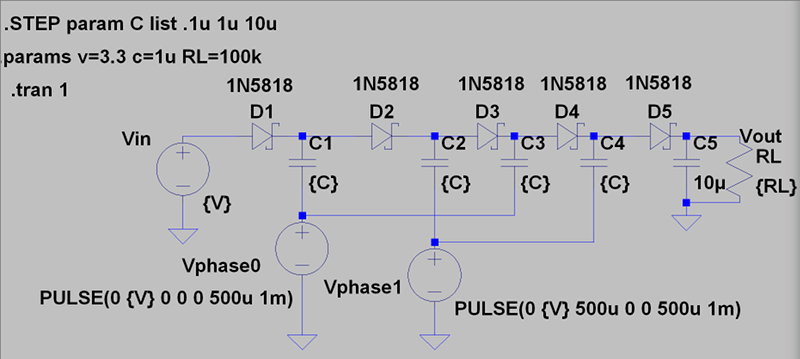
Vin is just the supply voltage: 3.3 V in this case. Vphase0 and Vphase1 are two square waves that are the opposite of one another. That is, when Vphase0 is high, Vphase1 is low and vice versa. These are probably outputs from a microcontroller, although it could be a 555 and an inverter or any other two-phase clock source you can dream up.
Consider the very first moment of operation. C1 is empty and Vphase0 is low. C1 will charge through D1 until it is at voltage Vin.
Then Vphase0 goes high. The capacitor stores energy so it can’t just go to zero volts across it like a resistor would. In fact, when we say C1 will charge to Vin, what we really mean is the voltage across the capacitor will charge to Vin. And since Vphase0 is now at Vin, the voltage across C1 is still Vin and so the voltage from the junction of D1, C1, and D2 will be twice Vin: Vin from Vphase0 and another Vin from C1.
The process repeats with the next stage. C2 charges to 2 x Vin while Vphase1 is low and then jumps to 3 x Vin when Vphase1 goes high. In theory, you could add as many stages as you like to get an integer multiple of your input voltage. The final capacitor, C5, doesn’t add any voltage because it connects to ground, but smooths out the output.
Reality Check
Of course, the reality is a little different. The diodes drop some voltage. I used Schottky diodes to minimize the effect, but still. The output square waves are not going to get all the way to the supply rail. The more current you draw, the more you are going to droop the capacitors when they are storing energy instead of charging and that’s going to affect the output, too.
So how bad is it? LT Spice can easily answer that question. If you haven’t used it before, LT Spice is a great adaptation of Spice which is well-known circuit simulation software. LT Spice is from Linear Technologies, but they offer it to the community without charge. You can download it from the Linear website. If you need a quick tutorial, we had one earlier you can check out, or have a look at the video at the end of this post. Although LT Spice runs under Windows, it works well on WINE so you can run it on your other computers, too.
Spice Tricks
It is really easy to just draw a schematic and simulate it. However, I used a few tricks to make things easier. C1 to C4 all have the same value and if you want to experiment with the values it is very painful to enter each one of them. The three voltage sources are the same, too. While there is only one RL, representing the load resistor, it is also a parameter you probably want to change during testing.
To make things easier, I didn’t assign specific values for these items. For C1 to C4, I assigned {C} as the value. This means somewhere else I have to specify a parameter named C. I also used parameters {RL} and {V}. If you look near the top left of the schematic, you’ll see a .params command that sets the three parameters. This makes it really easy to change things to try different scenarios.
The other nice thing you can do once you have a parameter is to sweep it to different values. That’s what the .STEP directive at the very top does. It varies C to three different values. You can also omit the LIST keyword and just provide a start, stop, and increment. For example, .STEP C 0.1u 1u 0.2u would cause the simulation to use 0.1, 0.3, 0.5, 0.7, and 0.9 as step values. Of course, you can remove the .STEP line if you just want a simple simulation.
Result
You can see from the results below that larger capacitors (C1–C4) help to a point. Of course, the bigger C5 and the higher RL, the longer it will take to charge to the final value. The green trace is the 10 μF run. The blue and red traces are for 1 μF and 0.1 μF, respectively.
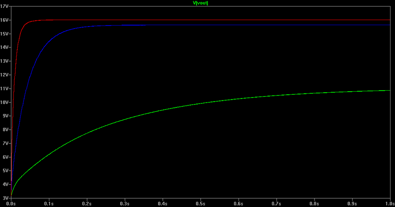
You’ll notice the period of both clock signals is 1 ms or 1 kHz. Each stays on for exactly half that time (500 μs) but Vphase1 has a 500 μS delay at the start. This is what keeps them out of phase. If you want to experiment with frequency, duty cycle, or rise and fall times, you can open those two sources and make changes. In general, higher frequency leads to better results and smaller capacitors, at least to a point. Parasitic capacitance is always a problem and gets worse as frequency increases.
You might also want to try different values of C5 or try replacing the diodes with ordinary diodes to see what that costs you. Of course, changing the load resistance to draw more current will change things. For example, look at the simulation below that uses .step param rl 1k 10k 100k.
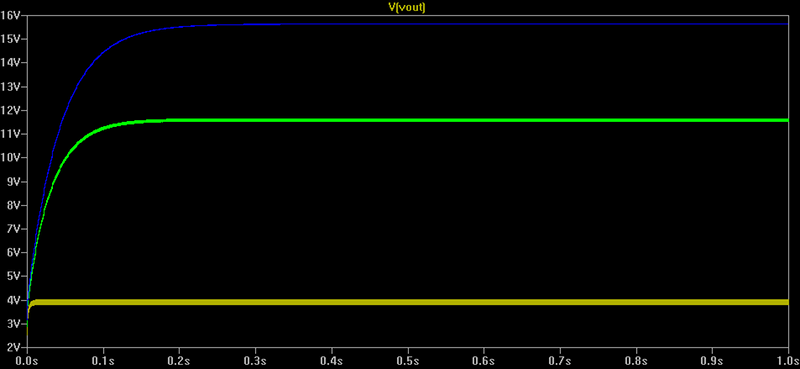
At 1 kΩ, you barely get any increase at all. The load is drawing almost 4 mA. With 10 kΩ you get between 3X and 4X multiplication. At 100 kΩ you get more than 4X. Try changing C to 10 μF and you’ll see better results. Or try 47 μF. You might also want to increase C5 at 1 kΩ to get better filtering. You can see how thick the lower traces are which is the unfiltered ripple.
Probably the best thing to do, though, is to simply probe different parts of the circuit to visually see how each stage builds on the previous one. Don’t forget you can measure currents, too, which can often provide insight into circuit operation. However, when using the .STEP command, you only get the nicely colored traces if you display only one value. If you add multiple traces, each family of traces will get a single color.
The Value
That’s the real value to simulation. A few minutes of playing with this circuit and you’ll have a feel for what parameters change the output. That incredibly valuable. Sure, you could breadboard the circuit and that’s probably the next thing you should do, but it isn’t nearly as time and cost effective as using a simulator like LTSpice when you want to tweak many parameters.
Is it perfect? No, a breadboard version will probably be a little different because I used ideal capacitors. If you right click on each capacitor and pick a model of an actual capacitor, you might notice some slight differences because the model takes into account parasitic resistance and other effects.
There are other techniques you can use to modify the Dickson charge pump. For example, on an IC, the diodes are likely to be MOSFETs. There are also variations that try to overcome the diode switching threshold or correct other undesirable effects.
One of the most interesting things about simulation like this is you can easily probe anywhere and quickly try out new ideas. Maybe you’ll come up with a new architecture for a multiplier and they’ll name it after you.


Outstanding article! Very well written and presented.
Extremely pertinent and usable.
I just used one of these connected to the end of a DC to DC converter to generate the voltage necessary for a transistor to avalanche in a Jim Williams pulse generator. It made a rise time so quick I couldn’t mearsure it with my new 350MHz scope.
I’ve been looking for a reference to an a good layman’s article (and/or articles) on avalanche in a bipolar transistor. Can you give us any help, including a reference to the Jim Williams pulse generator?
Many thanks.
http://www.siliconvalleygarage.com/projects/picosecond-pulser.html
https://www.eevblog.com/forum/projects/jim-williams-pulse-generator-is-still-strategic-military-or-dual-use-technology/
[PDF warning]
http://www.analog.com/media/en/technical-documentation/application-notes/an47fa.pdf?domain=www.linear.com
Thank you very much.
Seeds for exploration…
http://www.analog.com/media/en/technical-documentation/application-notes/an94f.pdf
http://www.analog.com/media/en/technical-documentation/application-notes/an47fa.pdf
…and thank you very much.
You can use a MOSFET instead of the diodes. Less voltage drop. http://www.ti.com/lit/an/slva139/slva139.pdf
No you can’t use FETs like that TI circuit. There are other circuits (e.g. https://www.researchgate.net/figure/N-stage-cross-coupled-Charge-pump-1_fig7_304346665) which use FETs as synchronous rectifiers but they are more complex.
Schottky diodes like shown here are quite good.
Yes you can use flipped direction n-mosfet’s with protection-diode going in the same directions as the above diode.
Just tie gate to the Source pin, much lower voltage drop as you are not just using the diode inside the mosfet..
Yes you can use flipped direction n-mosfet’s with protection-diode going in the same directions as the above diode.
Just tie gate to the Source pin, much lower voltage drop as you are not just using the diode inside the mosfet..
Useful circuit – fun to make really high voltage with. It looks like your voltage sources are “ideal”? Meaning no internal resistance. Typical microcontroller pins (or CMOS logic gates) have current limits and internal resistance. You can insert this into the simulation for a more realistic result as a series resistance between the voltage source and the caps. You’ll find the real world circuit’s ability to deliver any useful current is very dependent on how close to ideal the voltage source (micro or logic) is. A series resistance adds its own time constant to the circuit’s capacitor charge time – so the caps can take a relatively long time to charge and discharge compared with the drive frequency. In addition some pin drivers can be damaged if you pass to much current through them (source or sink direction).
+4
Or you could play around with this live like add an extra stage and change capacitor values, change the square frequency, or the duty cycle (if you don’t have the time to download and install spice)
http://tinyurl.com/yceab24e
http://tinyurl.com/yclvtdur
Shut up, you had me at LT Spice simulation!
Holy page break Batman!
If you are going to higher voltages:
C3 can be in series with C1 etc so that the capacitors don’t need to withstand the full output voltage.
I have made these that went up to the thousands of volts using waveforms at many 100s of volts as the starting point
It looks like the time-to-charge vs capacitor value graph is mis-described. You say that the green trace is the smallest caps, yet it show the slowest rise time…
You are right. I had a few versions of the graphics and I must have swapped the colors around at some point.
This is pure gold. Can’t wait for the new episodes!
Hope it gets really comolicated at the end.
Will be a fun drive.
Thank you.
Is any old diode ok? 1n4114?
probably going to use this on a raspberry pi pic programmer to get programming voltage (provided the 3.3v is sufficent to transfer the data to a 12f675)
Very nice, thanks!
One trick to minimize the diode drop over the entire chain is to place a single diode across the input and output as well with the Anode on the input and the Cathode on the Output. …. I used to race RC cars, and use this kind of charge pump for a turbo boost on the straight away …. here is a YouTube link to the circuit in action, the caps are 1000uF … https://www.youtube.com/watch?v=McPoNhNRIsw