
Today, SiFive has released two new cores designed for the lower end of computing. This adds to the company’s existing portfolio of microcontrollers and SoCs based on the Open RISC-V ISA. Over the last two years, SiFive has introduced a number of cores based on the RISC-V ISA, an Open Architecture ISA that gives anyone to design and develop a microcontroller or microprocessor platform. These two new cores fill out the low-power end of SiFive’s core portfolio.
The two new cores included in the announcement are the SiFive E20 and E21, both meant for low-power applications, and according to SiFive presentations, they’re along the lines of an ARM Cortex-M0+ and ARM Cortex-M4. This is a core — it’s not a chip yet — but since the introduction of SiFive’s first microcontrollers, many companies have jumped on the RISC-V bandwagon. Western Digital, for example, has committed to using the RISC-V architecture in SoCs and as controllers for hard drive, SSDs, and NASes.
 The first chip from SiFive was the HiFive 1, which was based on the SiFive E31 CPU. We got our hands on the HiFive 1 early last year, and it is a beast. With the standard complement of benchmarks, in terms of raw power, it’s approximately twice as fast as the Teensy 3.6, based on the Kinetis K66, a 180 MHz ARM Cortex-M4F. The SiFive E31 is about 1.5 times as fast as the Teensy 3.6 on a pure calculations per clock basis. This is remarkable because the Teensy 3.6 is our go-to standard for when you want to toggle pins really really fast with a cheap, readily available microcontroller platform.
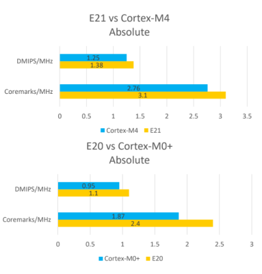
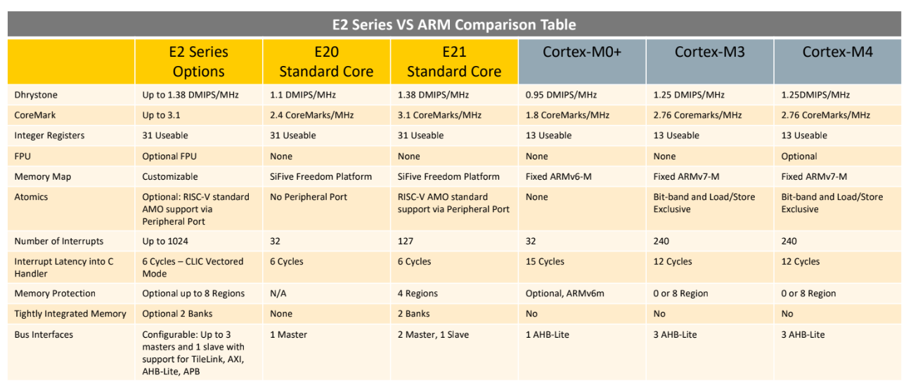
But sometimes you don’t need the fastest or best microcontroller. To that end, SiFive is looking toward a lower-power microcontroller based on the RISC-V core. The new offerings are built on the E2 Core IP series, with two standard cores. The E21 core provides mainstream performance for microcontrollers, and the E20 core is the most power-efficient core offered by SiFive. In effect, the E21 core is a replacement for the ARM Cortex-M3 and Cortex-M4, while the E20 is a replacement for the ARM Cortex-M0+.
Just a few months ago, SiFive released a gigantic, multicore, Linux-capable processor called the HiFive Unleashed. With support for DDR4 and Gigabit Ethernet, this chip would be more at home in a desktop than an Internet of Things thing. The most popular engine ever produced isn’t a seven-liter turbo diesel, it’s whatever goes into a Honda econobox; likewise, many more low-power microcontrollers like the Cortex-M0 and -M3 are sold than the newer, more powerful, and more expensive chips. Even though it’s not as exciting as a new workstation CPU, the world needs microcontrollers, and the more Open, the better.


Does the interrupt latency take register saving into account for risc-v core?
As there is 32 registers and no multiple load/store instruction, it means that if it’s not done by hardware you can have up to 32 cycles latency (depending on EABI), quite different from the 6 cycle figure given…
Just what I was about to say. The register file pushed by the m0/m3 matches pretty well the the C EABI. The cycle numbers given are more apple v dragon fruit comparisons. It is great if you are just doing port I/O in the ISR. But that isn’t inferred in the description of ‘getting to C’.
You don’t need to save all 32 registers, only the normal “caller-saved” ones.
The point the OP is making remains valid. Comparing their “6 cycles” with no reg saving is unfair to Cortex-M whose published latency of 12-13 cycles DOES include saving regs
Wrong. Interrupts may happen anywhere by nature – unlike entering/leaving functions which are predictable and so optimizable to save only the necessary registers. You must save ALL the registers you happen to use in your interrupt whatever their nature: caller-saved, callee-saved, temporary, even flags register if any because the interrupt is “interrupting” in the middle of the sequence of a function where temporaries shall still live when resuming the interrupted sequence. That’s the reason why some architectures offer shadow registers to avoid the cost of saving register when entering an interrupt and restoring then when leaving the interrupt.
Yes, but callee-saved are saved by the function, not by the ISR mechanism, so they’re normally not included in the entry time.
Short (leaf) functions will often manage to run entirely in the caller-saved (e.g. the argument registers on RISC-V calling convention) so this is actually a fair metric to use.
The time quoted is to get into a C function compiled with the “interrupt” attribute. That means the function itself will save only the registers it actually needs. A simple handler might only need to save one register.
If the interrupt handler function needs more extensive processing and calls normal C functions (i.e. without the “interrupt” attribute) then it will automatically save the volatile registers first. In the standard *nix ABI that’s a0-a7, t0-t6, and the return address (16 registers). An EABI is in the process of being defined. It’s probably going to end up needing to save 7 registers.
Note that a load/store multiple instruction makes your program smaller, but it doesn’t make it any faster. The same goes for hardware register stacking.
The Cortex-M also sets up nested interrupts in those same 12 cycles. It’s too bad the RISC-V designers never seem to have looked at what makes Cortex-M such an elegant microcontroller architecture. As it stands, it has all the drawbacks and awkwardness of MIPS32.
I’m guessing you haven’t read https://github.com/sifive/clic-spec/blob/master/clic.adoc and in particular section 6.3, which I think may address your concerns.
The CLIC is built into the E20/E21.
No, not really. The code shown uses load/store multiple instructions that I thought were very much left out of RISC-V. If they are disguised macros, then the “12 instructions” statement is a lie. In any case, the latencies look far longer than those for Cortex-M.
Those are not store multiple instructions. This is not assembly language source that you can actually assemble. You might notice that things such as “FRAMESIZE” and “OFFSET” need to be substituted with actual values (different ones each time in the case of “OFFSET”). Something like “sw t1-t6, OFFSET(sp)” is just shorthand for six different instructions with different offsets from the stack pointer.
Using the proposed EABI which has four argument registers a0-a3 and two temporary registers t0-t1, the actual code could look like the following:
irq_start:
#—- Interrupts disabled ———————
sub sp, sp, -48 # Allocate space on stack.
sw t0, 0(sp) # Save t0.
csrr t0, mcause # Get mcause of interrupted context.
sw a0, 4(sp) # Save a0.
csrr a0, mepc # Get mepc of interrupt context.
bgez t0, handle_exc # Handle synchronous exception.
sw t0, 8(sp) # Save mcause of interrupted context.
sw t1, 12(sp) # 1 more temporary to save
sw a0, 16(sp) # Save mepc.
sw a1, 20(sp) # 3 more arguments
sw a2, 24(sp)
sw a3, 28(sp)
sw ra, 32(sp) # 1 return address
csrrsi a0, mnxti, MIE # Get highest current interrupt and enable interrupts.
# Will return original interrupt if no others appear.
#—- Interrupts enabled ———————–
beqz a0, exit # Check if original interrupt vanished.
get_entry:
lw t0, (a0) # Indirect into handler vector table for function pointer.
csrrsi x0, mstatus, MIE # Enable interrupts (only needed for backwards branch here)
service_loop: # 5 instructions in pending-interrupt service loop.
jalr t0 # Call C ABI Routine, a0 has interrupt ID encoded.
That’s 18 instructions and 21 cycles before you’re in a standard C EABI interrupt handler function. That’s a little more than the 15 clock cycles for Cortex M0+, but the difference is not likely to be a major problem for users and it results in a very significant savings in gates, area, and power.
If more interrupts arrive at the same priority level before this interrupt returns then they will be chained at a cost of only 5 instructions and clock cycles.
Does it have port IO [like Intel] or is everything memory mapped [like ARM] ?
I mean the “callee-saved”, of course
“Just a few months ago, SiFive released a gigantic, multicore, Linux-capable processor called the HiFive Unleashed.”
As opposed to what? The Windows-capable?
As opposed to a microprocessor core that isn’t capable of running Linux and runs things either baremetal or on something like FreeRTOS?
ChibiOS that runs on the HackRF port-a-pack. There are many OSes other than just Windows, Linux.or OSX.
My preferred OS is OpenBSD for CARP alone it is worth knowing ( https://www.openbsd.org/lyrics.html#35 – ‘Left with little choice, we proceeded to reinvent the wheel or, more correctly, abandon the wheel entirely and go for a “hovercraft”.’ ).
As opposed to not being Linux-capable, smart arse.
I.e. it has an MMU and implements the privileged ISA spec.
Hi there!
Any reason why the Arm CoreMark/MHz results shown in the tables are much lower than the commonly measured ones and certified by EEMBC on real chips?
Typically Cortex-M0+ is measured at 2.3-2.46CM/MHz and Cortex-M4 in the range of 3.4-3.5CM/MHz.
And about the comparison E31 with a M4F, looking briefly at the spec it’s much closer to a M7 or even probably a Cortex-A! A look at the spec unveil “40-entry branch target buffer (BTB) which predicts the target of taken branches, a 128-entry branch history table (BHT),” that will be massive once casted in a chip.
Instead of offering “replacement” of 10 years old cores, what about getting something really new and innovative? ;-)
Thanks for your insight,
Scott
Like the “Mill architecture” ?
Like that will ever leave vaporware status.
I can’t see any reason why it would not go into full production.
With very low volume MOSIS orders ( https://www.mosis.com/products/fab-processes ), it is not like it is impossible to achieve. As time goes on it will only become easier and cheaper for people to develop their own chips, if they want.
It’s been fifteen years and AFAIK they still haven’t got a running implementation.
@asdf It is not like the RISC-1 CPU with only 44,500 transistors, which took 4 years with a massive team, and that was mostly removing parts from an fully implemented and tested preexisting design, and adding lots and lots of registers. The Mill is different. I can see why they would want to dot their I’s and cross their T’s, to locked down everything they can. That and the core development team is tiny.
Nothing runnable includes an FPGA prototype. By this point it’s just a hype machine for spending VC money. If there are any genuinely useful ideas, they’ll be picked up once they have to sell the patents for cash.
@asdf
Why would they publicly demonstrate a FPGA prototype ? They have filed patents, are working in the background while waiting for protection to stop rivals from stealing their work and leapfrogging them. Lots of features of the architecture is just pure genius. It will scale extremely well, there are so many good things about the design, I don’t understand your negativity.
https://patents.google.com/?assignee=Mill+Computing%2c+Inc.&num=25&sort=new
They posted on their own forums that they’ll do an FPGA implementation first. I’ve seen enough of supposedly revolutionary projects that either go nowhere or turn out to be pretty mundane not to jump on the hype train. The proof is in the pudding, I’ll wait until they have something to show, but I’m not holding my breath.
When they are taking on a $200 billion company with a long history of dirty tricks ( https://www.youtube.com/watch?v=osSMJRyxG0k ), I can see reasons for not exposing innovation without having major protections in place.
Ivan Godard must be another fan of 5D chess.
One really hard part is the compiler, until it is ready the hardware is completely useless. Even if the last the patents were all granted tomorrow and Mill released a fully working FPGA bitstream, there is still very little that could be done with it. It is a totally different beast compared to anything else. Having a variable length instruction set, and processing two half-bundles of instructions at once, one heading up in address space and the other down. Executing a peak of 33 instructions every cycle. There is nothing that is totally crazy in the design everything is based on novel use of existing technology. They are well inside the existing limits on bus transfer rates, SRAM cache sizes. They are not trying to do anything nuts like trying to increase the cache size by factor of 10. Everything that they are trying to do from a silicon standpoint is totally possible, it is just so much different than anything else out there that will add inevitable delays in bringing to market. There are risks, but I personally do not see it as vaporware, if 3 years after they have been granted all their patents they do not have a range of products, then I would change my tune. VC’s would hold back the bulk of funding until all patents have been granted.
As of May 8, 2018, they have been granted 14 patents, I think it is running silent.
I personally feel that the need in today’s world for replacing these cores cannot be overstated.
Technology is advancing at such a rapid pace with private research and manufacturing that competition is nearly impossible, whether from competitor companies or open groups. This locks control of the technology away from consumers and independent developers and engineers. Being able to recreate the feats of engineering that are processors and other silicon designs in a way that escapes the corporation-only limitation of NDA and “copyrighted” designs allows us to see what is actually going on in our devices, allows individuals to learn more and therefore be able to innovative from new knowledge and improve existing designs, and allows companies and individuals to use open and freely available designs which would otherwise be blocked behind a paywall. This allows for more innovation from the market. The most important benefit, in my opinion, is that we can see what is going on in the same way as software and recreate it for educational or practical purposes. Now, for a departure: I’d like to say text editors are the microcontrollers of text processing software. Microsoft Word is more like a pc processor. There are other oddball variations, like table managers such as excel, database managers, lyric editors, messaging programs, and many other things that could be considered as text processing software. Imagine if only large companies had the ability to make these. You wouldn’t see innovative messaging programs, open solutions like LibreOffice, cloud services like Google docs, or one-off projects like Billy Average’s hit-song-generator-that-i-coded-in-a-day-for-fun. If you’re familiar with vim and emacs, imagine if no one could make their own branch of the software or contribute to the existing project, or if no one could look at the code to understand strange behaviors. Or, worse yet, if no one could look at the source to verify that there wasn’t spyware or adware.
Note: I wrote this in one go and didn’t try too hard to make the allegory accurate or all that well-written. Try to get the gist and work with that.
If you buy a RISC-V processor, you still can’t “see what is actually going on” inside it. An implementation of the RISC-V ISA (because that’s what it is, a specification) is just as easy to backdoor as an implementation of any other instruction set. Even if the manufacturer releases what they claim to be the source files of the design, the only way to verify that is by de-capping and reverse-engineering the chip on a transistor level, and that’s extremely time-consuming even for very simple devices.
RISC-V is also hardly the first of its kind, it’s just the most hyped one. Western Digital using it in their devices doesn’t move the needle much, hard drive manufacturers have used all sorts of controllers before without anyone caring much.
The CoreMark figures shown are measured on real hardware using the same gcc version and flags (e.g. -O2) on both systems to have an apples-vs-apples comparison.
ARM’s published figures are based on the IAR compiler, which is much better than gcc.
IAR have announced they are working on a RISC-V compiler that is expected to be in beta before the end of the year.
Realistically, RISC-V gcc is currently pretty new and immature compared to ARM and the generated code has a lot of obvious opportunities for improvement.
I want give a shoutout to GAP8 SOC from greenwaves technologies it is 8+1 core chip with RISC-V CORE + custom extensions for DSP and Hardware Convolution Accelerator available as tangible silicon chip.