When it comes to inspection of printed circuits, most of us rely on the Mark I eyeball to see how we did with the soldering iron or reflow oven. And even when we need the help of some kind of microscope, our inspections are still firmly in the visible part of the electromagnetic spectrum. Pushing the frequency up a few orders of magnitude and inspecting PCBs with X-rays is a thing, though, and can reveal so much more than what the eye can see.
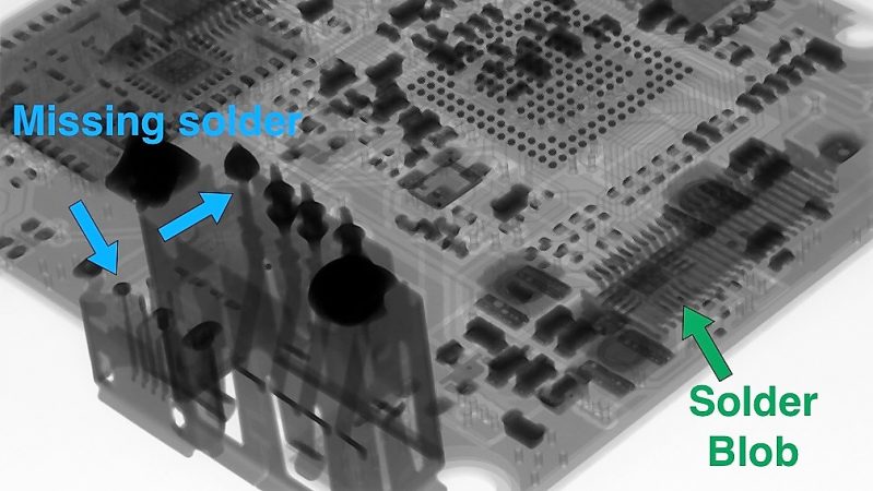
Unlike most of us, [Tom Anderson] has access to X-ray inspection equipment in the course of his business, so it seemed natural to do an X-ray enhanced teardown and PCB inspection. The victim for this exercise was nothing special – just a cheap WiFi camera of the kind that seems intent on reporting back to China on a regular basis. The guts are pretty much what you’d expect: a processor board, a board for the camera, and an accessory board for a microphone and IR LEDs. In the optical part of the spectrum they look pretty decent, with just some extra flux and a few solder blobs left behind. But under X-ray, the same board showed more serious problems, like vias and through-holes with insufficient solder. Such defects would be difficult to pick up in optical inspection, and it’s fascinating to see the internal structure of both the board and the components, especially the BGA chips.
If you’re stuck doing your inspections the old-fashioned way, fear not – we have tips aplenty for optical inspection. But don’t let that stop you from trying X-ray inspection; start with this tiny DIY X-ray tube and work your way up from there.
Thanks for the tip, [Jarrett].


I (briefly) worked for a company that made these X-ray microscopes trying to design a cheaper X-ray source tube. They use very hard and intense X-ray sources compared to medical imagers. Which isn’t to say that you couldn’t hack your own system from discarded dental equipment. Though it might be unwise :-)
If it’s cheap you’re after, ditch the tube and use a radioisotope…good ol’ Cobalt 60 is fairly simple (read cheap) to make – simply put you just chuck a piece of Cobalt 59 (the stable natural isotope) into a reactor for some time…
1.17 MeV and 1.33 MeV is plenty of energy for PCB inspection, probably even massive overkill…might be a good use for “spent” Co 60 sources that are no longer adequate for their original purpose.
Radioisotope won’t work for this application. As there is no such thing as an X-ray lens you need to use a pinhole camera (in reverse), and the resolution of the image is governed entirely by the size of the point source.
They use a very thin layer of tungsten on a beryllium window and a very focused electron beam so that the emitting region is a few microns wide and a few microns thick. I think that a radioisotope of those dimensions would be far too dim an emitter to be useful. (but I haven’t done the calculations)
Beg your pardon?
https://en.wikipedia.org/wiki/X-ray_optics
OK, so there are ways to focus X-rays. I was (slightly) misled when I was taught Physics 30 years ago.
But I don’t think that any of those methods are suitable for Co60 X-rays (1.17 & 1.33MeV) on the scale that would be practicable for an X-ray microscope. Certainly none of them seem _easier_ than an X-ray tube..
I read somewhere about a theoretical x-ray laser that would use zone plates and diffraction optics to focus the beam. Problem was, the zone plate array that served as a lens was to be located a few light-seconds away from the radiation source, which happened to be a phased array in which each element was a precisely-timed hydrogen bomb floating in space. Of course, why not?
The cold war was a strange time. Probably out of a hobbyist’s reach :)
+1
I wonder if my dentist’s x-ray device could also do this. (one with a move-able arm). I might have to become friends with mine! :)
It’s possible with some of the equipment at least, but I’m unsure if it’s even practical…
https://www.raspberrypi.org/blog/x-rays-no-specs-required/
He could have used a Supermicro board instead and look for the spy chip embedded between the layers… ;)
+1
As it was used to find (an) existing fault(s), I suppose there is/was no danger in harming the silicon wafers with the X-Rays?
Wait, people don’t actually think cheap chinese wifi cameras are built with quality, do they???
But to be honest, that board actually looks quite good fro a $25 WiFi. Try putting your DSL or Cable modem under x-ray if you really want to see some scary joints.
The write-up is done very well. Great detail and I absolutely love the overlayment of the schematic on the power supply circuit. That is brilliantly done.