Creating A Game Boy ROM From Pictures

There are very few legal ways of obtaining ROM files for video games, and Nintendo’s lawyers are extremely keen on at least reminding you of the fact that you need to own the game cart before obtaining the ROM. With cart in hand, though, most will grab a cart reader to download the game files. While this is a tried-and-true method, for GameBoy games this extra piece of hardware isn’t strictly required. [Travis Goodspeed] is here to show us a method of obtaining ROM files from photographs of the game itself.

Bits can be manually edited to fix detection errors.

Of course, the chips inside the game cart will need to be decapped in order to obtain the pictures, and the pictures will need to be of high quality in order to grab the information. [Travis] is more than capable of this task in his home lab, but some work is still required after this step.

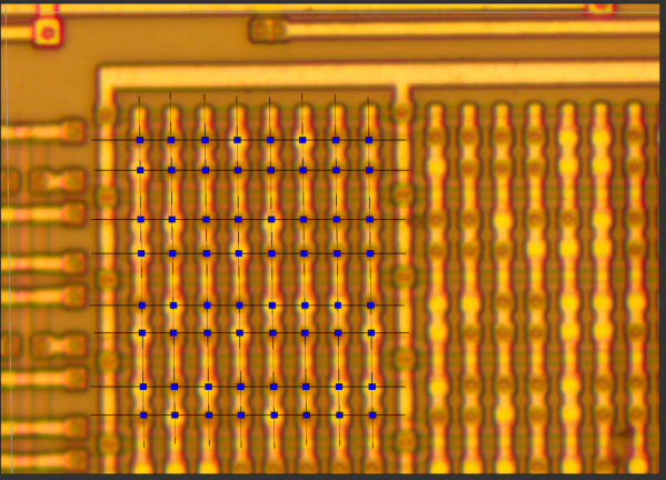
The individual bits in the Game Boy cartridges are created by metal vias on the chip, which are extremely small, but still visible under a microscope. He also has a CAD program that he developed to take this visual information and extract the data from it, which creates a ROM file that’s just as good as any obtained with a cart reader.

This might end up being slightly more work especially if you have to decap the chips and take the photographs yourself, but it’s nonetheless a clever way of obtaining ROM files due to this quirk of Game Boy technology. Encoding data into physical hardware like this is also an excellent way of ensuring that it doesn’t degrade over time. Here are some other methods for long-term data storage.

Seeing A Webcam’s PCBs In A Whole Different Light

When it comes to inspection of printed circuits, most of us rely on the Mark I eyeball to see how we did with the soldering iron or reflow oven. And even when we need the help of some kind of microscope, our inspections are still firmly in the visible part of the electromagnetic spectrum. Pushing the frequency up a few orders of magnitude and inspecting PCBs with X-rays is a thing, though, and can reveal so much more than what the eye can see.

Unlike most of us, [Tom Anderson] has access to X-ray inspection equipment in the course of his business, so it seemed natural to do an X-ray enhanced teardown and PCB inspection. The victim for this exercise was nothing special – just a cheap WiFi camera of the kind that seems intent on reporting back to China on a regular basis. The guts are pretty much what you’d expect: a processor board, a board for the camera, and an accessory board for a microphone and IR LEDs. In the optical part of the spectrum they look pretty decent, with just some extra flux and a few solder blobs left behind. But under X-ray, the same board showed more serious problems, like vias and through-holes with insufficient solder. Such defects would be difficult to pick up in optical inspection, and it’s fascinating to see the internal structure of both the board and the components, especially the BGA chips.

If you’re stuck doing your inspections the old-fashioned way, fear not – we have tips aplenty for optical inspection. But don’t let that stop you from trying X-ray inspection; start with this tiny DIY X-ray tube and work your way up from there.

Thanks for the tip, [Jarrett].

Easier PCB Vias With Drill Trick And Conductive Ink

If you’ve ever made double-sided PCBs without professional equipment, you had to deal with connecting one side of the board to the other. You have a few obvious choices: 1) Rely on component leads to connect both sides (and solder both sides); 2) Create vias and solder wire to both sides of the board; or 3) Use through hole rivets. [Diyouware] had a different idea: use conductive ink. After a few false starts, they found a technique that seemed to work well.

This isn’t the first time we’ve heard of people trying conductive ink with varying degrees of success. The biggest problem, usually, is that the ink wants to run out of the hole. [Diyouware] has an interesting solution for this problem: Don’t drill the hole all the way thorough.

Continue reading “Easier PCB Vias With Drill Trick And Conductive Ink”