
We’ve reduced printed circuit board design to practice so much that we hardly give a thought to the details anymore. It’s so easy to bang out a design, send it to a fab house, and have ten boards in your hands in no time at all. All the design complexities are largely hidden from us, abstracted down to a few checkboxes on the vendor’s website.
There’s no doubt that making professional PCB design tools available to the hobbyist has been a net benefit, but there a downside. Not every PCB design can be boiled down to the “one from column A, one from column B” approach. There are plenty of applications where stock materials and manufacturing techniques just won’t cut it. PCBs designed to operate in space is one such application, and while few of us will ever be lucky enough to have a widget blasted to infinity and beyond, learning what’s behind space-rated PCBs is pretty interesting.
Getting There
The design of PCBs for use in space is primarily driven by the two main phases of spaceflight: getting there, and being there. Some missions will eventually return to Earth gently, of course, and some will set down on the surface of another world, but for the most part, we blast them up and they stay there for the rest of their useful life.
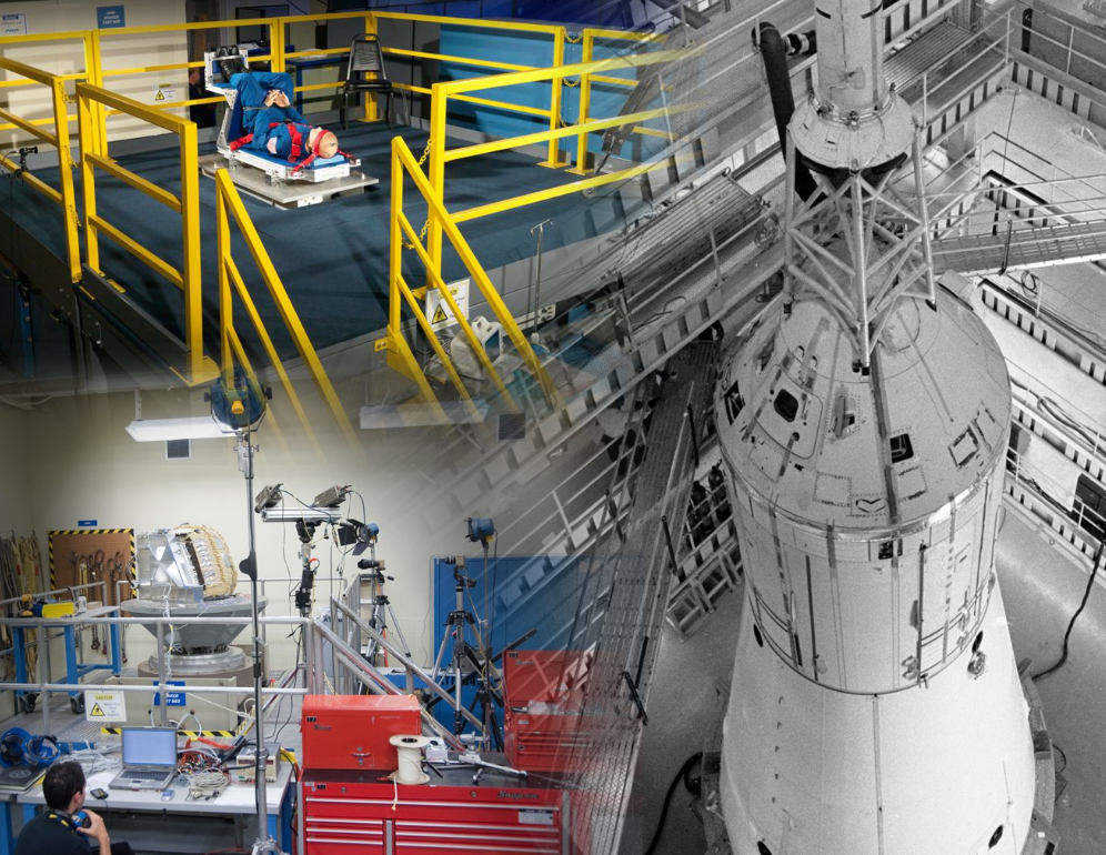 During the short trip to space, the primary challenge to any PCB in the spacecraft is vibration. The PCB will be in close proximity to a barely controlled, continual explosion contained by a machine that’s made to be as light as possible, and even with shock-dampening mounts between the vehicle and the payload, vibration can be significant. NASA’s vibration testing facilities can impart enormous forces to huge loads over a range of 5 Hz to 3 kHz, and blast test samples with acoustic energy up to 167 dB, to simulate what payloads will experience during launch.
That means the PCB has to be built from materials that can withstand a far more dynamic environment than the most stressful situations for earthbound equipment. Somewhat surprisingly, NASA’s own PCB working group guidelines list many common substrate materials, like glass fiber and phenolic resins. It does list a number of more exotic materials, like Kevlar, Teflon, and various resins. For most applications, NASA seems to prefer polyimide substrates, which will be familiar to anyone who has ordered a flexible PCB. The Kapton film upon which these are built is a polyimide, and NASA uses flexible and semi-rigid PCBs built from the stuff regularly. When a design calls for a rigid PCB, polyimide reinforced with glass fiber is sometimes used as well.
Regardless of the materials uses, designers often deal with the physical abuse of launch in the simplest possible way: making the PCB thicker. This only works up to a point, though, since payload weight translates directly into launch costs. When launches go for upwards of $20,000 a kilogram, adding a few grams of weight to a board has to be considered carefully.
Being There
Despite their magnitude, the duration of the stresses introduced during launch are short-lived, and if the payload survives the short ride into space, it will face a whole host of challenges over its service life that PCBs on the ground rarely have to consider. Chief among these is outgassing, or the tendency of materials to release gasses when placed in the vacuum of space. The resins used in PCB substrate that are perfectly stable under atmospheric conditions may quickly bubble out of the board once in space, which can lead to contamination of other surfaces and weakening of the substrate. Where outgassing needs to be controlled, substrates of PTFE resins with glass fiber reinforcement manufactured under stringent conditions are often used.
 Few earthbound devices will experience the thermal regimes that something in orbit will, and those thermal loads are a major design consideration for space-rated PCBs. Without an atmosphere to moderate temperature swings, one side of an orbiting satellite can be scorching hot in the sun, while the other side plunges to frigid temperatures. The physical stress introduced by thermal expansion has to be dealt with; again, this mainly boils down to choosing the right substrate material, and closely matching its coefficient of expansion to that of the metal used for plating. This minimizes the physical stress on the traces and on through-holes.
It’s also important to consider how temperature affects the electrical properties of PCBs. The dielectric constant of the board material changes with temperature, and the designer needs to take that into account, particularly in RF circuits where intrinsic impedance is critical. Dielectric considerations are also important given that PCBs in space often encounter high-voltage electric fields due to solar activity. Boards need to handle those charges without breaking down.
All things considered though, printed circuit boards for space applications are remarkably similar to their terrestrial counterparts. We’ve learned a lot about dealing with the extra challenges of space, and space agencies like NASA as well a numerous commercial interests have developed the tools needed to ensure that one simple mistake doesn’t scrap a multi-billion dollar asset before it can start returning on its investment.


if the main issue for pcbs is the vibration, then give it no room to vibrate, simple.
although this may cause some Tetris style problems in the designing process
The problem is that everything flexes a little bit and assembled cards have little room for flexing. You basically need to stake everything down and torque all screws down to spec. For example, large BGA parts are rarely used due to having such a large area that cannot be flexed. They will use the column version, CGA, instead since the columns allow for a little bit of movement.
Not so simple.
Everything is a spring. Everything. That 100mm length of pcb between two mounting studs? A spring beam with a resonant frequency determined by the pcb material characteristics, the thickness of the pcb and the mass of attached components. Halve the distance between mounting studs to 50mm? That resonant frequency doubles. It doesn’t however, disappear. You could keep going until the board is continuously mounted along its length. You’d still have a spring beam across its width. Clamp the board along all four edges, you still have a 2 dimensional spring beam across the middle. Mount all components topside and glue the entire bottom surface to a mounting plate. Now you have to ensure that the thermal characteristics of the pcb and that mounting plate are sufficiently close so to prevent differing expansion rates popping the glue loose – or worse – doing the very thing you’re trying to avoid, fracturing a pcb track or solder joint. If you can manage that, you will still have a spring beam that will vibrate, now consisting of the pcb and the mounting plate assembly. Its resonant frequencies will be different from the 100mm-spaced stud-mounted pcb, as will its strength and weight. Many factors are using during design and test to ensure that the solution best fits the mission requirements. Critical navigation systems will have different requirements than an ancillary system.
I’ve only written about board vibration, but every component on that board is also a spring beam or pendulum with its own vibration characteristics. It is common today for avionic designers to use Finite Element Analysis software to evaluate designs for airworthiness.
This subject really isn’t so simple.
Simple in theory, much harder in practice. I
Go study the design of a IBM AP-101 Series avionic computer – they’re ancient but still used in our military aircraft. They’re built like tanks and so are the circuit boards which range from 8 to 11 layers.
The whole system was designed to handle a harsh environment and constant vibration, not just for a few minutes but hours and and hours on end.
If the PCB can’t vibrate, then the variety of masses mounted on it which ARE vibrating will rip themselves off. Fully potted assemblies are a weight cost. Shock mounting and careful design saves a lot of money in the long run.
Boards are the easy part. Designing your hardware around outdated rad-hard parts is the hard part.
I thought the trend these days is to just accept the risks and use COTs parts, but of course you’ve designed your system with sensors, multiple power planes, multiple ground planes, A/B routing of signals, etc. Or just building a pair with some failover controls. Getting parts RAD hardened isn’t as useful any more since regular stuff is now pretty darn tolerant. Love to learn more.
You need rad hard when the vehicle is exposed to cosmic radiation, i.e. no longer in Earth orbit. Part of the cosmic radiation is energetic enough to cause permanent changes to the silicon crystalline structure. As these changes build up, the electronics slowly die. Redundancy doesn’t help because multiple units will all accumulate damage at the same time. Shielding doesn’t help either, because the radiation is powerful enough to go through any kind of affordable shielding.
True, but again, not all missions are interplanetary, and have a much lower budget than the flashy too-big-to-fail-just-send-more-money scientific missions.
Cosmic Radiation is still very much in play even while you are in Earth Orbit.
Rad Hard parts are hardened against effects such as:
Total Dose which is cause by ionized particles
Displacement damage (the crystalline structure)
Charging Effects
Single Event Effects cause by heavy ions (commonly considered to be Cosmic Rays)
You can shield (and all spacecraft do) against Total Dose and Displacement damage, however for Single Event effects, you need to use part that have known ‘Safe operating biases”, or known upset rates, and account for them in your design.
So if shielding doesn’t work and cosmic rays are causing permanent changes to the silicon, how does one radiation-harden a semiconductor device at all?
How is it doable at all? Silicon-on-Sapphire wafers for the integrated circuits, that I know of.
For analog systems, use materials like GaAs and GaN that are inherently rad hard.
For digital systems, triple mode redundancy. Build your design in triplicate for critical parts and vote on the outcome of logic. If there is a transient that causes a bit flip, you can just ignore the result that is different than the others.
You make the silicon so thin that disruptive collisions become extremely unlikely.
You can look up info about how Intel worked over their Pentium class chips for rad resistance. Simple things such as larger die features help.
I’m not so sure that redundancy won’t help, since a single cosmic ray won’t hit both systems unless you’re really unlucky. And if you’ve designed a third/fourth reset circuit out of basic components, that does a full reset in those cases, you should be ok. Henry Spencer wrote some stuff on how they designed the MOST experimental satellite using COTS stuff. Fascinating design info. It would be great to get Henry to contribute here….
In Low Earth Orbit (LEO), the earths magnetosphere provides a lot of protection. You can use a lot of parts that would fail instantly otherwise.
Is it possible to emulate the magnetosphere? Create a large EM field around the skin of the satellite?
From memory, that’s how old watches were protected from EM fields.
Wat
On paper it is not impossible. But the power required to produce a high enough Lorentz force to deflect ionizing particles travelling at nearly the speed of light and provide the same level of protection as earth is just astronomical. And deflecting a large number of ionizing particles means that you will need additional shielding because of Bremsstrahlung. But the power level required means that is may as well be impossible, it is only possible on paper if you totally ignore reality. The idea is about as practical as this – https://medium.com/our-space/an-artificial-martian-magnetosphere-fd3803ea600c
Actually I’m wrong, the Bremsstrahlung term only applies inside of atoms. Anyhow if charged particles are captured by the magnetic field and spiral they would loose energy and the amount of energy lost would produce photons which could be gamma rays, X-rays, UV, visible light, ….
It depends on what’s being built. It is true that the Cubesat industry is driving the need for the use of commercial off the shelf parts, because their designs are low cost, low earth orbit, and short life span.
However, the traditional Space Industry is still quite risk averse, and RAD Hardened parts are still very much a requirement.
You can throw most COTS stuff in LEO and have it work fine for a bit. Anything in GEO needs to have some sort of radiation hardness assurance whether that’s through buying parts that have been tested by the manufacturer, NASA, or another agency or you can test your unit on the system level at a particle accelerator for SEU tests and sit it next to Co-60 for total dose tests.
Well the alternative is to use modern day chips and encase them inside very large blocks of lead that have sat at the bottom ocean for a hell of long time (e.g. https://www.nature.com/news/2010/100415/full/news.2010.186.html ). Basically you need high quality shielding that will not cause what you are trying to prevent by adding shielding.
10 microns (1971 – each trace was ~50,000 silicon atoms wide)
1 micron (1985 – each trace was ~5,000 silicon atoms wide)
90 nanometers (2004 – each trace was ~450 silicon atoms wide)
10 nanometers (2017 – each trace was 50 silicon atoms wide)
7 nanometers (2018 – each trace is 35 silicon atoms wide)
Having really old tech in space, means that the odd stray bit of radiation will not toggle random gates on and off, and make the equipment useless. In reality it is a numbers game: 10 stray electrons in 1970’s or 1980’s technology would have minimal effect, but in the latest and greatest technology it is a problem.
Yes with enough of the right kind of shielding (and associated higher launch weight costs) we could have the very latest technology in space. But the cost benefit calculations, currently yield older technology as the cheapest solution for the overall best average performance and the highest rate of return on investment. Until that changes or we make a new breakthrough and develop an economical atom isotope sorter, that allows us to make cheaper higher quality shielding, I don;t see anything changing.
No, you can just make shields out of a layering of tantalum and copper. These both provide excellent shielding and weigh much less than a block of lead.
https://www.designworldonline.com/using-tantalum-to-protect-critical-electrical-components/
Thanks, that is a very interesting material, with a lower overall mass, but a higher overall volume to achieve the same level of attenuation.
So in many ways it is similar to laminated bullet proof jacket (Graded-Z shielding) vs a sheet of steel (block of lead)
I’m guessing electrolytic capacitors are a no-go as well (boiling off electrolyte in vacuum).
I’ve used tantalum caps.
Anything that’s prone to leaking electrolyte would be unwelcome, yes. Aluminum polymer capacitors are excellent, though: https://nepp.nasa.gov/files/24294/CARTS2012_Liu_Reliability.pdf
Wonder at what point it’s easier to keep the electronic’s pressurized (tho I’m sure that would the temp swings even more interesting to deal with)
I’m not going to say that electrolytics are a good idea, but they’re in sealed containers.
If the electrolyte is able to boil because you removed atmospheric pressure, the part already had a problem.
The selection of electrcal/electronic/electromechanical (EEE) components is a big task in it’s own.Most commonly there is a list of approved parts that can be used. Anything not on the approved list needs prior approval for use.
The PCB may need to be designed to sit in a warehouse in a tropical region for some years before a launch can be scheduled. (At least that was my experience.)
And people are contemplating putting man on mars. Tssk…
Downright shameful, yes. Why are we still contemplating?
If we’d pushed for Mars with the same vigor that we pushed for the moon, the colony there would have multiple voting precincts by now.
Sign me up. First flight. Let’s go already.
If we had pushed for Mars with the same vigor that we pushed for the moon, we would have a few dozen dead astronauts, and a public outcry that would shut the program down.
We still don’t even know HOW to run the tests, that can help design systems, that can help keep people alive in TRANSIT.
And even if we HAD that nailed down, we don’t have the orbital assembly station to make the transit craft. Which is a whole program in itself.
We don’t even know what it will take to set up a moon colony yet. A Martian colony is literally impossible to do safely.
I have never designed for space, but I had a boss in a prior company that came from NASA. He explained that one of the primary problems in putting boards on the ISS is the fact that components, and you gotta give us some leeway here because we were in the chip-making business, so… He said that components, especially chips, would outgas toxins that cannot be had in an enclosed environment such as the ISS. These chips had to be packaged in non-outgassing materials like ceramic. I imagine the same can be said about passives on the board as well.
Only if the outgassed toxins can reach the life support system. Of course, having electronic parts surrounded by rocket fuel brings different problems – I need to watch Apollo 13 again.
But why would plastic chips outgas? In all manned flights, because of humans stubborn refusal of survival in vacuum, there is a pressurised cabin. And for electronics not under pressure, it does not matter, because there won’t be any human there. And if it not because of the pressure, then what would cause the outgas?
Things can still outgas under atmospheric pressure. Leave out a cup of water and it evaporates, not as fast as it would in a vacuum, but it still happens.
This minimal outgassing is probably fine on earth with plenty of fresh air, not so much in a sealed craft,