Designing circuit boards for high speed applications requires special considerations. This you already know, but what exactly do you need to do differently from common board layout? Building on where I left off discussing impedance in 2 layer Printed Circuit Board (PCB) designs, I wanted to start talking about high speed design techniques as they relate to PCBs. This is the world of multi-layer PCBs and where the impedance of both the Power Delivery Network (PDN) and the integrity of the signals themselves (Signal Integrity or SI) become very important factors.
I put together a few board designs to test out different situations that affect high speed signals. You’ve likely heard of vias and traces laid out at right angles having an impact. But have you considered how the glass fabric weave in the board itself impacts a design? In this video I grabbed some of my fanciest test equipment and put these design assumptions to the test. Have a look and then join me after the break for more details on what went into this!
What I Mean By “High Speed”
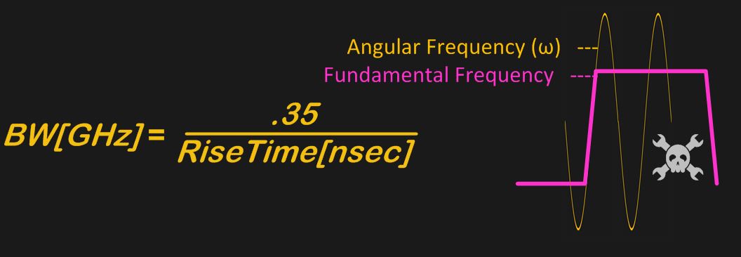
The term “high speed design” can mean different things to different people depending on what they are used to working with, but for me it’s where the energy of the rising and falling edges of the signals dominate the behavior compared to the fundamental frequency of the signal itself. In other words a 10Mhz signal that has a 1ns rise time has a bandwidth of roughly 350Mhz as seen by the formula below. Ultimately it’s the energy in the rise/fall time of the signal that affects a lot of the design.
The relationship between the bandwidth and the rise time can be approximated as:
With regard to high speed design rules, my first rule of thumb is to be cautious about rules of thumb. I use rules of thumb as an early estimate that helps me to get an idea of how all of my design rules and goals play together.
As someone who has been doing design since the 1970’s I have seen the evolution of assumptions and design guidelines mature and it’s fair to say that there were a couple of things that we got wrong along the way, some things almost comically wrong. For example, I have heard people say that electrons slam into each other trying to turn corners at high speeds so it’s a bad thing to do, we now don’t think that way.
High Speed Design Assumptions
Some of the principles of high speed design are listed below. I can’t get to all of them in this one post but I do want to get to all of them in turn.
- At high speeds it’s all about the propagation of the Electro-Magnetic (EM) field, not electrons.
- High speed current follows the path of least impedance on a power or ground plane, not the path of least resistance.
- Due to the geometry of the glass fabric weave used in the construction of the PCB, the impedance of a signal trace may change based upon the orientation and the position in relation to the weave.
- Right angle corners in PCB traces may not be near as detrimental as often assumed.
- In a properly designed multi-layer PCB, the placement of decoupling capacitors near the loads may not be near as critical as is assumed.
- Ferrite beads in line with the various voltage traces may do more harm than good.
- Differential pairs aren’t coupled to each other like we often depict, their return current is through the ground plane, not through the other half of the pair of traces.
- Tightly coupling a differential pair may not have as good of noise rejection as two random paths provided they are the same length.
- Since the current flows on the surface of a conductor (known as skin effect) high speed PCB’s may specify smooth or polished copper traces for the inner layers so that the path is smoother and straighter.
EM Fields
At high speeds it’s not so much about the flow of electrons but rather the energy in the Electromagnetic (EM) field and the way those fields propagate. Yes some electron displacement occurs along the way but a simple way of looking at this statement is that all of this works in a vacuum.
If you were to picture multiple traces in the same dielectric space you can see that the fields would overlap and consequently interact with each other. This is one of the primary causes of crosstalk. Another way of saying this is that crosstalk occurs in the whitespace between the conductors where the fields overlap and interact.
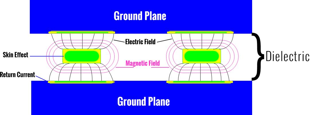
A function of thinking of signals and their EM fields racing around is that the return current follows as closely to the outbound signal as possible. Last time I talked at length about the fact that the path of minimum inductance is the path that forms the smallest loop between the outbound and return currents. Consequently this means that the return current follows the path of least inductance, hence the path of least impedance (Z). Impedance is the combination of resistance(R), inductive reactance (XL) and capacitive reactance (XC) all measured in Ohms (Ω)


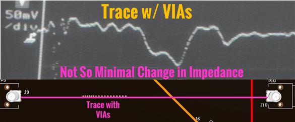
The image on the left above shows the return current density follows the signal on a single layer. In real life, signals often jump layers and in order to have the return current continue to follow the signal closely (and therefore control the impedance) we have to place VIAs nearby that connect the internal reference (ground or power) planes. This is shown on the right.
Impedance Testing
To continue testing some of my design rules listed in the beginning I built a PCB to test the impedance of different PCB traces.


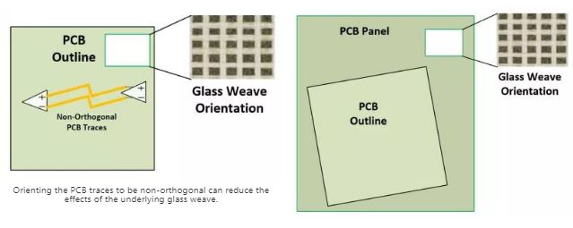
PCBs are constructed of layers of conductors (typically copper) and dielectrics (typically epoxy coated glass fibers). As speeds go up these materials become more and more specialized. Since the glass fibers or weave are uneven, they can have an effect based upon how the conductors interact with the weave of the fibers as shown below.
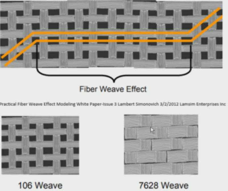 Simply put, traces that align directly with the row of the glass fibers will have a different impedance than the trace that experiences alternating bundles of fibers.
Likewise a trace in the vertical direction will see a different amount of glass under it than a horizontal trace due to the differences of the weave density in different directions. One answer is to spread the fibers out during PCB fabrication, but as you might expect, the price of the completed PCB starts going up.
One way to test the impedance of a PCB trace and to see changes along the path, is a high speed Time Domain Reflectometer (TDR). TDR’s are commonly used at slower speeds as in cable testing, [W2AEW] has a very informative video on the whole theory behind it.
High Speed Time Domain Reflectometer
Behind the technology is a fast rise time pulse. I had actually started to write this post as instructions on how to make a fast rise time generator using various techniques after reading Jenny List’s article on pulse edges. During my research I bought a pulse generator that clocked in at 32 picosecond (ps) rise time (sold as 40ps or faster) designed by an engineer named Leo Bodnar. When I received my pulse generator I saw that Leo had used a venerable piece of equipment known as the Tek CSA803/SD24 Communications Signal Analyzer (CSA) which has a 20Ghz bandwidth and a 17.5 ps rise time pulse to characterize my module. I just had to have one of these CSA’s myself and watching eBay got me a good find, though I haven’t told my wife yet. With this new-to-me piece of equipment I set off to test how easily I could see the effects of the glass fiber direction on impedance.
Horizontal vs. Vertical PCB Traces
As can be seen below there is a definite difference in the baseline impedance based upon the direction of the PCB trace. See the video for all of the fun in setting up for these pictures.
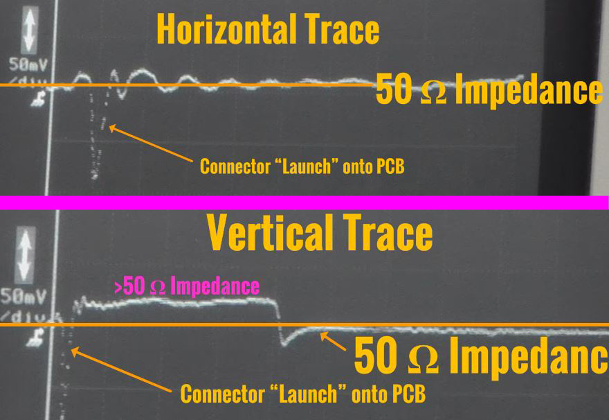
You can see a definite and measurable difference in the impedance of the traces based upon the orientation of the trace on the board, in the case of this board the Vertical trace was off by approximately five percent.
There are a couple of techniques that help deal with this effect without the cost of going to a more expensive PCB with a tighter glass weave. My CAD software supports the two main techniques shown below to help automate the process but both can be done manually as well. The first technique entails zig-zagging in a not-so-orthogonal way in an effort to statistically reduce the effects. If there is the option of laying out the PCB in a larger panel then it can be cocked to one side (I have heard 10-11 degrees but it is affected by other variables as well) so that again the sum of signals running down the worst case paths is minimal
Shocking Discovery: Square Corners Probably Don’t Matter
One of the factoids that plague the industry is the concern about what the effect of right angle corners used on PCB traces might have on the impedance of those traces. Other complaints are that the RFI emissions are higher with right angles and that acid can build up in the corners during the fabrication. I will put this board on the spectrum analyzer and check for “EMI spray” in the next video post and if your PCB fab house complains about acid in the corners then I would humbly suggest that one find a different fabricator.
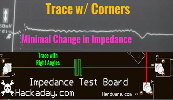
I set out to see if I could detect the effects of corners myself with my new 20Ghz capability. As seen above the effects of right angle corners at 20Gz (.35/17.5ps=20Ghz) with a trace width of 5.27mil (calculated for 50Ω Impedance) on the characteristic impedance are minimal.
Square Corners Mean More Capacitance, but Not Much
At the heart of the debate over square corners vs. angled corners is the slight change in capacitance due to the change in trace width represented by a square corner.
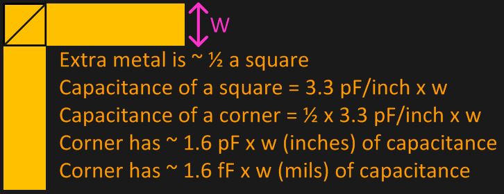
We know the capacitance of the area of the metal since we are talking about 50Ω impedance in general. Per the equations above a 6mil trace would have an additional capacitance of 9.6fF (femtofarad), or 0.0000000096 μF, this is really small. The other thing that minimizes the effect of the corner is just how fast it goes by at the velocities we are talking about, which are sizable fractions of the speed of light. Given that a signal travels 6 inches in 1ns on a standard FR4 PCB, the signal will get through the corner in 30ps. (Which is why I have to use equipment with a 17.5ps rise time to examine it)
More about this can be seen in Eric Bogatin’s post on EDN where he comes up with a nice rule of thumb:
- If your rise time is 10ps, don’t worry about corners unless your 50O line widths are wider than 50mils.
If concerned about corners on your design, ascertain what your bandwidth is (35Ghz for 10ps rise time) and your trace features, given that 50mils is really big for a signal trace, it is more like a power trace in most designs.
Just for the Heck of It.
Just for the heck of it I ran the same test only instead of corners I had “hanging VIAs” which admittedly are worse case as they are like little capacitors and antennas hanging off the trace. I wanted to be sure to have something that would show up as an example of worse case when compared to right angle corners and this example did not disappoint.
Conclusion
The point I really wanted to get across is to be cautious when considering rules of thumb type advice. Question the sources of information, and do not be afraid to measure for yourself what you can when you can if in doubt. Above all else ask the question, “How do you know?”.
As these results were all demonstrated in the “time domain”, I will be demonstrating some of the aspects of the “frequency domain” as it relates to high speed design in the next installment.


The “connector launch” impedance mismatch there is probably because the ground layers aren’t cleared around the center conductor on the inner layers: the pad adds way too much capacitance. Generally if you just clear the inner layers a little bigger than the pad and have a solid plane on the bottom layer, that tends to work pretty well. If you want to be insane, Intel/Altera’s got a detailed document on the half-through hole/half-SMD connector layouts and how much clearing you generally need.
Depending on the connectors used it can be a pretty big hit if you don’t compensate for the excess pad capacitance, even at way lower frequencies than you’d expect (~200 MHz).
“Per the equations above a 6mil trace would have an additional capacitance of 9.6fF (femtofarad), or 0.0000000096 μF, this is really small.”
Obviously that depends on the trace width needed: a 6 mil 50 ohm trace is pretty rare for a 4-layer board. That’s one of the reasons why I like PCBWay, because their 4-layer stackup is *really* rare: the top/bottom prepregs are *crazy* thin. A 2-layer 62-mil PCB really wants well-matched edges.
But you’re totally right, worrying about square corners is generally a waste of time. Especially if you’re not worrying about capacitance compensation for series components – those virtually always dominate.
But the “test board” you have isn’t that great for testing some of those other assumptions, like the differential pair testing – that specific stackup has the ground *so close* that it’s impossible to couple differential pairs stronger than they’re already coupled to ground.
Agreed. I hope to show some things about stackup in the next post to include thinks like the trade-off between signal-to-reference plane spacing vs VCC/Ground reference planes spacing, I.E. SI vs PDN. It might prove a little tough to get across as there are a dozen way to bake a cake and same with opinions on the ultimate stackup for different situations.
The clearout issue you mentioned also applies t series caps or terminations resistors. I didn’t worry about it here as teh launch made it easy to show the start of the important part of the trace easy to show on camera.
Altera has pretty good guidelines for PCB layout though they still say to put a ferrite inductor in series with some VCC connections which is proving to be more problematic than originally assumed.
Samtec is also one of my goto’s for connector SI guidelines.
“Altera has pretty good guidelines for PCB layout though they still say to put a ferrite inductor in series with some VCC connections which is proving to be more problematic than originally assumed.”
I think most people’s problems when adding ferrites along the power planes is that “ferrite” isn’t actually a generic component. I don’t use ferrites that don’t have SPICE models, and I’d prefer them to have full S-parameter characterizations up through 1 GHz. Ferrites are really fairly complicated parts, and so the manufacturer recommending “cap + ferrite + cap” is really a recipe for disaster, because you probably don’t know what cap or what ferrite was used. They really should be specifying recommended attenuation at certain frequencies, or VCC frequency/noise masks (much like phase noise masks that certain manufacturers give on clocks).
Steve Weir has a great presentation on this from 2009, but it’s partially lost to the depths of time (search for “Understanding Ferrite Beads and Applications 2009 weir ipblox” and you should be able to find copies of it). He’s got more recent talks on it too, although I always think he complicates things a little bit too much. It’s great to have full PDN simulations for everything, but usually cap + ferrite + cap + (5x cap+series resistor) will work well.
… That being said, it’s usually easier and about the same cost to just to throw a feedthrough cap (“three-terminal capacitor”) filter on the rail, unless you *really* need 40-60 dB filtering.
Thanks for the link and agreed on characterization of ferrite.
The growing criticism of inline inductors is why put a low pass filter in line with a component with high speed current needs. It may reduce the symptom but by starving the part of current when the real issue is that a lower impedance power supply is needed. A PDN with no inductance and unlimited current would not need a ferrite, so how to get there in real life is the challenge. With that said, ferrites are still great for stripping noise off signals headed for the connectors, etc.
Lee Ritchey in his books “Right the First Time” talk about this, and shows the impact ferrites have on high speed eye diagrams (think 16 through 64gbps) and he mentioned that the bigger FPGS’s PLL’s wont even work correctly with the impedance of a ferrite in the VCC supply (I assume that current starving would result in phase jitter noise)
Thanks for your feedback! Bil.
Awesome. Next 25 minute installment please!
The test pattern for square corners looks like there could be quite a bit of capacitive coupling between the traces. I’d expect it to work very much different than a normal trace with a square corner, which does not turn back on itself. The test results tell nothing about square corners in normal traces, though I agree with the conclusions.
This a standard constant length function built into my Altium CAD, and so I assume that the math isn’t horrible in it’s effect. Since the capacitance isn’t a lump sum but continuous I would expect more of a loss of definition on the wave front (emphasis) than a self resonance created by the inductance/capacitance, but I haven’t run the math or a simulation.
Heh, if the geometry is good enough for DDR4 design I would think its not horrible.
The self-capacitance is going to be pathetic compared to the added inductance of the accordion, especially considering how tall they are.
But really that just stresses that the overall result is correct: if you don’t screw the impedance up enough to see it with a giant accordion with lots of edges, you’re not going to see it with a single one.
Agreed. Its all tradoffs. When I zoom way in on the CSA you would think corners and vias are completely unusable if not taken in the larger context. At the end of the day a serpentine intensive layout like DDR4 needs a healthy simulation pass for the reasons you mentions.
So would I still use a beveled corner? Sure if it doesn’t hurt anything layout-wise, but I am not going to freak if I forget to run the beveling pass on a normal speed board, or worry about them ever on an I/O line. I was just disusing with an old friend a very old PCB that would not have been routable using bevels due to space constraints.
So here is something I didn’t have time to bring up: Why are teardrops/fillets really used on traces entering pads?
“Why are teardrops/fillets really used on traces entering pads?”
Why are they *really* used? Because some layout packages allow it to be done automatically, that’s why. :) There are actually quite a few reasons that I know of, though: increased mechanical attachment strength from the trace to the pad (*ridiculously* important if the board’s going to be possibly reworked by hand, especially if possibly not by professionals) is probably the best reason.
The goofy argument that people use sometimes is that it’s a smoother impedance transition. And obviously a smooth transition to a pad *can* have a smoother impedance transition (it can in fact have *no* impedance transition if you do it in CPWG and the component allows for it) but that’s not going to matter until *extremely* high frequencies. And if you’re working at those frequencies, you aren’t using the teardrop/fillet that the layout software produces anyway.
Hey, Bill Herd, if you read this, I see you have a Hewlett Packard 3314A function generator. It has a cool easter egg that my dad wrote into the firmware: https://www.davmar.org/hp3314a.html which is pretty easy to demo.
I have a pile of them. They’re fun.
Ha! That’s really cool. I love Easter Eggs like this and having you pop in and share the story of your Dad being the one behind it makes me smile. Bil, you should play the Easter Egg as and outro for a future video :-D
Yeah I love that little generator, I have simulated ultrasonic systems with one of those in lieu of a custom processor assembly (okay the 3314A IS a custom processor assy but you know what I mean) . I will have to check out the egg!
It is interesting and has been designed on high speed PCB but another great idea for generating the register write clock signals for Running the microcode latch at twice the speed of PHI2: http://forum.6502.org/viewtopic.php?f=4&t=6282&start=15
Corners matter where I work! we have 60ps risetime 2kV 100ns pulse width TLP’s!
I used to repair TV’s where you could see coronas from the 28KV especially around sharp points and also I hung around the local AM station with the RF power amplifiers, yes they matter then. Funny to think that it won’t arc unless you don’t clip the wire correctly (I kept a small smoothing file in my tools) These examples may have been the start of the myth of corners at low voltage.
And this anecdote brings the expression “corner cutting” into a new perspective :-D
My experience with > 25Gb/s was that I needed a low loss dielectric, smooth copper and the PCB panel was rotated 15 degrees wrt the PCB blank.
Bits are about 6 mm long! (for Er = 4.)
Worked first time, but we did get a very expensive consultant to run a 3D EM sim on the vias and connector.
Heh, I hand drew the EM fields since I don’t have an expensive 3D field solver. I think a repeatable scenario is to get something like a Nelco PCB with spread/rolled fibers though I don’t have current costs for doing that. The concerns is that something changes in PCB fab that changes the effectiveness of the layout. (Ideal angle now 12 degrees instead of 15 for example) Like everything its a trade-off.
I had to cut out the part about skin effect and smooth copper. I hope to get to them during on eof the PCB related followup videos… there was just too much in this one and something had to be cut. (Its why you see skin effect mentioned in the drawing)
Great comment about the length of a bit, I can also picture the drag of the dielectric as if you were moving your hand through water.
Excellent write up, at first I interpreted the title as fast design process as in advanced s/w Ai etc, glad I took a closer look. All you wrote totally missing and not even touched on in any practical sense at all when I was at uni late 1970’s. Thanks for the effort and detail, cheers
Thanks Bill! You covered a lot of issues I try to bring up to younger engineers about what they should always be aware of at a macro-perspective when it comes to signal integrity and best practices. When I write high level code, I’m always thinking of the instruction sequence the compiler will generate for each statement – that influences how I write the high level code. Same with hardware. When laying out a trace and surrounding ground, I’m always thinking of how the forward and return paths will affect the waveform – which influences the layout. The first pass in school always starts with the ideal functional results. And most stop there expecting the real world to teach about real worlds. :)
Kudos.
Heh, because I came from the days of limited registers in the processors I too think in terms of the underlying code and how it gets implemented. Thanks!
It was my understanding that the rule of thumb against square corners was more about ensuring a good yield in manufacturing boards rather than anything electrical.
Yep, I have heard that and they used to say “acid in the corners”. My response is that if ever a fab house tells you that you should get a new fab house. I asked this question of someone intimately familiar with PCB fab over the last 30 years and he said that it was never really a problem.
The teardrop fillets were supposed to help with mis-registration of the drill hole in a pad but these days if a vendor cant hit a pad with a drill then how are they going to do micro and buried vias, let alone things like via in pad.
Thanks for the response!
I feel like getting flashbacks of my CID and CID+ certification lectures. :)
Very interesting topics and i like the way to try to break the complex down into a simple, understandable and even practically verifiable problem. Can’t wait to see and read more!
Thanks!
Good to see “advanced” topics covered on Hackaday, because modern jellybean logic is fast enough to cause problems for the unwary.
If you are prepared to tolerate a 3cm distance resolution, then you can use a much cheaper 1970s vintage portable TDR, the Tektronix 1502 (N.B. not 1502B, not 1502C, not 1503). The 1502 has a 140ps system risetime.
There are many 1502s on fleabay, but rarely do you see a working example. They have a strange PSU that requires functional NiCd batteries, some caps can leak and destroy PCB traces, and the tunnel diode can be damaged by any external voltage – hence the special shorting BNC connector. But if you can find a working example, they can give useful results and the vintage sampling scope can be hypnotic to watch.
And if you are really adventurous, you could reseal it according to the service manual, then operate it in rain and store it under water.
The place I got the CSA803 from replaced the battery for me before shipping. Its one of the few components that when you design it in you know for certain you are using something that will fail in 8 years or so. There’s a bunch of youngsters that give me crap that stuff I designed 35 years ago breaks from time to time, and then they tell me how they would have designed it better, including making better chips. :/
Thanks for debunking at least some of the advice I received while doing, as a complete newbie, the Gigatron PCB layout. I already had the impression that a lot of the “advice” and “rules” you find on websites, forums and youtube are more old wives’ tales than anything else: lots of handwaving, repeating of others and very little qualitative underpinnings of most of that. Still, I really -like- 45 degrees corners and we sprinkled way too many decoupling caps all over the place. But that’s also to preempt getting those tales thrown at us. (In reality the board works fine without any caps).
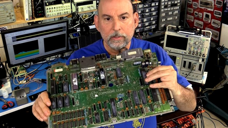
Only emission-wise, uhm well, lets say it’s a bit vintage in that regard. Any idea when inner ground planes became a common thing? Did the C128 have that for example?
No the C128 was one of the last of the two layer, at least for Commodore and we pushed it further than we should have (4 layer was just so expensive), I was lucky that we did not have memory corruption with just the addition of one wire. At million piece quantity the smallest violation gets amplified and things fall on the floor remarkably fast.
Basically when IC packages and memory got denser they had to go somewhere, hence 4 layer. It took a while to break the habit of trying to still use the inner layers as partial signal layers, and I have been guilty of that myself.
Yes 45 degree look cooler, and radius even better. And again I would not use them, but we don’t need to, especially for I/I lines.
Thanks for sharing your really cool anecdotes. It’s amazing how quick and how risky the design cycles really were back in the day, given the slow flow of knowledge and information. But perhaps the lack of Internet distractions and need for self-dependency speeds some things up as well…
I rarely break 16MHz myself, but I find myself hanging around the Microwaves101 encyclopedia and forums from time to time, just because it’s fascinating to see how the fast kids really live. It’s a different regime up at 77GHz!
The Autobahn of microwaves.
Ah, but what is your rise time of your 16Mhz signal? ;) That’s where the high frequency energy is.
For anyone further interested in this, I recommend “Transmission lines, antennas and wave guides” by King, Mimno, and Wing. It was first published in 1945 based on material for the military during WW2.
Yes, most of what we have known for 60-80 years is still valid, though some new materials help. I think Nylon was what broke open much of radar’s capabilities, which I believe is one of the reasons nylons were so hard to get as depicted in the movies of the day.
Interesting article, I didn’t know about the glass weaving effects.
BTW, the CSA803 looks really cool. Is it possible to build such an instrument DIY? For the last few weeks I’ve built a fast 25 MHz datalogger for up to 8 analog channels and 64 optionally additional digital inputs, with a DE10 Nano board, see here:
http://www.eevblog.com/forum/projects/4-channel-adc-10-mhz-8-bit-design/msg2075176/#msg2075176
I guess if I add a very fast sample-and-hold circuit in front of the analog inputs, controlled by the FPGA, it should be possible to use the slow ADCs (25 MHz max samplerate) to measure repeating signals with a very high analog bandwidth. Wouldn’t matter if I need to measure 1000 cycles, all a little bit phase shifted. I could generate the phase shifted trigger signals for the sample-and-hold circuits (I hope) and stitch it all together (this part should be easy) with the FPGA.
The real trick is to get the raw bandwidth. If you were to use a 40ps risetime pulse like the off the shelf part I found, you would need a Bandwidth of 8-10Ghz (10GZ ~ .32ps like I had). At these speeds the PCB’s don’t look like PCB’s like we are used to working with, they look like Microwave stripline with very strange devices soldered in in funny ways. (also I use a anti-static strip when connecting since ESD protection would ruin the bandwidth or be very expensive.)
So if you had the amplifier/front end that was good to these speeds, you could use a high speed sample and hold function and then a much lower speed A/D device, a signal wiggling within the capture window can screwup the reading, (see posts like https://hackaday.com/2016/05/05/analog-to-digital-conversion/ ) For me to do it right, I had to resort to the CSA, its like you would need the CSA to troubleshoot anything you would build or you would not know if everything is working correctly without something fast enough to compare it to.
You are right about the phase shifted sample times. I thought I had in the shower was that the sample times could even be random if you had a source of true randomness.
I was just pricing out high-speed PCB’s made with Rodgers RO0435 material and the price was a significant portion of the cost of a CSA off of Ebay, lol.
Right, probably very hard to design such a board with all the RF components and layout black magic. And I guess the jitter of the FPGA wouldn’t allow to use it to generate the trigger impulses for the sample and hold circuit, even if I maybe could create signals with phase shifts in the picosecond range by manually placing the LUTs with the FPGA floorplan. Interestingly the samplingrate of the CSA803 is only 200 kHz and the ADC has only 8 bit resolution. So if someone would manage to build such a frontend, the rest would be easy and such an instrument could be even done with the integrated ADC of a modern microcontroller.
Found a nice article about a project which has 3 ps sampling time:
https://publikationen.bibliothek.kit.edu/1000064176/4004863
But it uses a 16 layer Roger 4003C PCB, so just for the price of the PCB you could buy a CSA803 with all channels and extras installed from eBay :-)
How does your random sampling idea work? You would need to know somehow the time of each sample to reconstruct the original signal, and then you would have the same jitter problem of the FPGA, now at the input.
Eric Bogatin brought up the 8 bit resolution thing at the Altium conference where I met him and it turns out to be true on most scopes. He started by talking about the graticule, there are 7 major divisions. In each is 4 marks for a total for a total of 40 divisions in the vertical range counting the top and bottom and the axis themselves. That’s 6.4 levels between each minor graticule in a 256 level/8 bit scale. His point was you could not even see 6.4 levels between the small divisions with the human eye. This was a face palm moment for me as I always looked at resolution as a min S/N thing, not a “what can I discern on an oscilloscope face” type thing.
Also yes on the time between sweeps, but as long as you know accurately just when the sample occurred then you can build a picture. The CSA has a persistence mode and a color persistence mode that I didn’t even need as 200k is 3k samples every 60th of a second. I plan on using the color persistence mode when I show an eye pattern for HDMI in a future video.
Yes, my opinion is it is that sampling head and it’s bandwidth is where the magic juju is. My SD-24 cost almost as much as the CAS frame, but well worth it given in included the pulse generator also, and the backplane trigger path. They have a 50ghz head that I drooled over that I don’t need, but I drooled none the less.
Good talking to you Frank!
This is the best article I have read on here in a long time. Really great. I would be interested to see more on what effect impedance has on high speed signals and whether field solvers are really accurate simulations of the real thing. I had long heard about the square corner issue but always found it hard to believe that electrons care about whether a corner is 90 degrees or multiple 30 degree corners. Seemed unlikely to me, because sharp corner or smooth corner matters only if you have momentum (which requires mass, less mass less momentum). The magnetic field would of course be different but in a complex board the interaction between all those fields seems more important to me and hard to know without accurate (expensive) simulation of the entire system.
Supposedly an early “expert” likened a corner like a bunch of ping pong balls all slamming into each other trying to get around the corner. If we think of the field though which is only energy, then it can snap around the corner like the bikes on the original Tron.
So electrons do have mass, in fact I looked up how much last night (9×10⁻³¹kg) as part of the argument that electrons don’t make the full trip at .6 of the velocity of light, though they are displaced in the process. I am going to have a physicist doublecheck me but it takes 78.3kev to accelerate the mass of an electron to half the speed of light. That sounds like an improbable thing with a total potential of 3.3eV but again I am going to have someone check me.
In the old old days before I knew better I thought that a certain amount of energy radiated off of the end of a trace that turned a corner as I had been taught about antenna end effect, I didn’t account for the difference between the fact a dipole terminates into free air (377ohm) whereas a trace is still a trace and the signal just follows it.
For the next one I want to talk about PCB stackup and the power delivery network of multilayer boards and how to calculate decoupling and impedance, not just use rules of thumb.
Thanks for the feedback!
The electrons aren’t going “round corners”. (Hint: work out the average velocity of an electron going through a 1kW kettle. I think you will be surprised at how slow it is, i.e. <<c :) ).
What is "going round the corner" is the electric and magnetic fields.
Bogotin's rules of thumb (mentioned in the article) are worth knowing and understanding. Start at 0 and work up to 32 :)
https://www.edn.com/collections/4435129/4/Bogatin-s-Rules-of-Thumb
For a differential pair, why the return current is through the ground plane, not through the other half of the pair of traces?
I will talk about that more in a future video but the as I also don’t believe that the “common mode” rejection of having the traces track each other does what people think it does. Basically the important thing is that the two edges arrive at the same time as the circuit is really a crossing edge detector not a differential amplifier.
So two points about your question: The virtual coax, or transmission line is formed between the ground plane and signal not between the two signals. You could eliminate the other signal and the first signal would still go racing down the board with it’s impedance defined by its coupling to the return plane. The signals travel at the same time for both traces, if it was a return path the the signal would first go down one and then come racing back up the other, it doesn’t they both propagate down at the same time.
Picture the termination resistor at the far end. The center is grounded, even if isn’t shown as the center of it will stay near a ground potential (I don’t actually mean 0v level, I mean a grounded non-moving value), With that point grounded both signals goes racing down (remember, EM waves, not electrons) coupling to their respective return planes and then meet (hopefully at the same time give or take) at the ground reference in the termination resistor.
Again I will try and explain more in a future video as I have gotten this issue more wrong then right in the past.
Interesting. Bill, you are sort of right, sort of wrong. In the world of high speed signal integrity, it all depends. Feel free to contact me. I know a few things.
Scott McMorrow
CTO Samtec Signal Integrity Group
Thanks for doing a test board and using ebay stuff. It makes me want to set up an impedance analyzer to see how my PDN
really is on projects. It’s great to see someone talking about Bogatin.
Also, the “50 cal” comment cracked me up.
BTW, my first PC was the ViC-20, so Commodore has happy memories for me. Please post more stuff!!!!
-Will