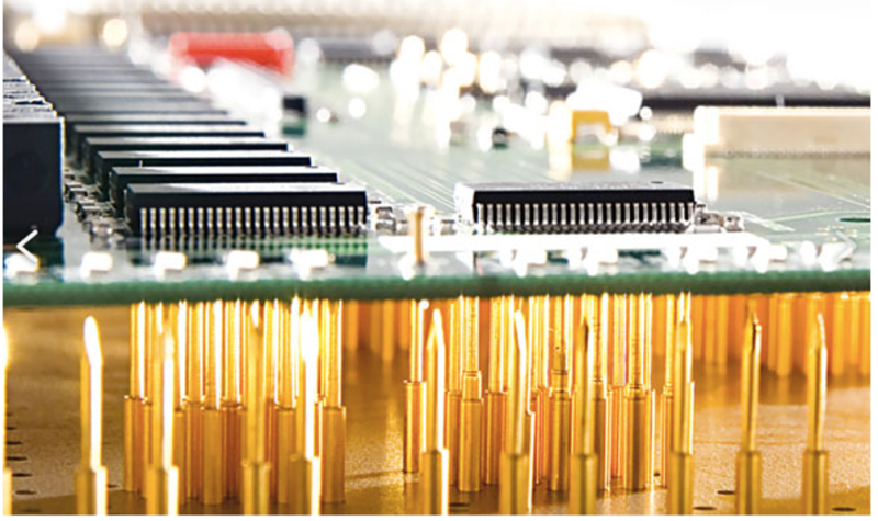
While it might be tempting to start soldering a circuit together once the design looks good on paper, experience tells us that it’s still good to test it out on a breadboard first to make sure everything works properly. That might be where the process ends for one-off projects, but for large production runs you’re going to need to test all the PCBs after they’re built, too. While you would use a breadboard for prototyping, the platform you’re going to need for quality control is called a “bed of nails“.
This project comes to us by way of [Thom] who has been doing a large production run of circuits meant to drive nixie tubes. After the each board is completed, they are laid on top of a number of pins arranged to mate to various points on the PCB. Without needing to use alligator clamps or anything else labor-intensive to test, this simple jig with all the test points built-in means that each board can be laid on the bed and tested to ensure it works properly. The test bed looks like a bed of nails as well, hence the name.
There are other ways of testing PCBs after production, too, but if your board doesn’t involve any type of processing they might be hard to implement. Nixie tubes are mostly in the “analog” realm so this test setup works well for [Thom]’s needs.


Pro-tip: design through-hole test points in your pcb that can be populated with pogo pins. That way you can use an otherwise unpopulated pcb with those pogo pins as a perfectly-aligned bed of nails.
Sadly, this may make the board much larger due to the holes. The alignment is usually solved by inserting a plastic board (such as POM) with precisely drilled holes between the DUT and the PCB beneath.
Normally, if i have to pogo sime boards, i resort to http://www.merifix.com/ quite fast. Had good success with their work. Cheap.
Yes! That works well. I have done that.
“the platform you’re going to need for quality control is called a “bed of nails“.”
its called ICT and can be done with a bed of nails or flying probes and its a mostly outdated practice in volume production
What’s the modern practice?
Can you elaborate on the reasons for “outdated practice”?
It has been replaced by “flying probe” machines. They land probes on components and can perform any measurement you want. Voltage, resistance, crosstalk, etc.
https://www.youtube.com/watch?v=lSNI2OTGOEE&t=1m7s
What is your reference for your opinion of ICT or Flying Probe being an “outdated practice”? I was at the IPC APEX Expo 2 weeks ago and saw at least a dozen offerings of the latest machines for both methods. I work for a CM and we use both on a routine basis for state of the art products. The Jabil Nypro plant in Porterville, CA was being auctioned off last week and 4 very used HP 3070 ICT machine were going for well over $40k the day before auction close with numerous bidders.I am pretty certain that both ICT and Flying Probe test methods are still very active.
I think one of the newer methods is to have a gazillion more pins, like a “brush”, and then characterise a ton of impedances between various pins for one board, and then compare that characterisation profile with successive boards. In other words: the system works automatically, you don’t need to give it any information about the board.
Please correct me if I’m wrong, then I’ll update my understanding.
This technique goes by a few names, but can also be done using flying probes – this removes the need to create the bespoke bed of nails fixturing. The impedance measurements are taken initially between each net and a single reference net (normally a 0V of some description).
It’s not “outdated” at all. There are simply more options right now. Each with their pros and cons.
Try telling a board stuffer that you want to flying probe your 20,000 expected annual usage product instead of building a fixture.
I’ve gotten complaints about a product I designed that is only ~2000 EAU.
I guess I reread your comment and noticed that you weren’t saying what I thought you were saying :).
Other than maybe Xray, what else makes ICT outdated?
pro-tip: make sure the force applied on the PCB is straight down, even small forces along the horizontal plane will increase failrate and ware down the needles.
make sure to add holes/indents for guidance pins.
google ICT testing and you will find more on this subject. posted some links (awaiting moderation)
see
https://www.electronics-notes.com/articles/test-methods/automatic-automated-test-ate/ict-in-circuit-test-design-for-test-guidelines.php
https://www.google.com/url?sa=t&source=web&rct=j&url=https://courseware.zcu.cz/CoursewarePortlets2/DownloadDokumentu%3Fid%3D114866&ved=2ahUKEwjb-4Gjwq_gAhWK2aYKHWkKAYQQFjAAegQIBRAB&usg=AOvVaw2Xyh05dFFDWyNd5nC-xaY7&cshid=1549745163668
I’m an old in-circuit (bed of nails) Test Engineer. For years – from the very late 1970’s to far into the Surface Mount era, In-circuit was THE test platform for circuit cards. Companies like ZEHNTEL, Teredyne and others designed and manufactured ICT or In-Circuit Test platforms and they all used bed of nails type fixtures. We used an assortment of ZEHNTEL 410 and ZEHNTEL 810 testers in our shop. The 410’s had HP desktop computers with HP Basic while the 810’s has X80 computers loaded with UNIX.
Early ICT test sets came out with guarding, a technique that mostly zero out parallel paths. Also, with some test sets you could use a mix of AC and DC signals to measure parallel caps, resistors and inductors, but the technology was not perfect. We were doing good if we got 80% coverage on a given board.
ICT test sets and bed of nail fixtures are still popular today but HP 3070’s seemed to be the survivors. A lot of pin through hole boards are still being manufactured and even SMT (Surface Mount Technology) boards are tested on ICT testers. But with SMT, the designer has to plan for bottom side access.
Because of accessibility, the modern equivalent is a Flying Probe Tester. Early Flying Probe technology came out in the late 80’s and Flying Probe technology has advanced quite a bit.
Interesting.
Thank you for sharing you knowledge!
Really lucked out on a purchase from one Chinese supplier. Bought 100 “PCB drill bits” for just a couple of bucks. When they arrived they were actually precision cross point head micro spring loaded PCB test bed pins. Gold plated with carbide tips. Instantly ordered a second batch, although I did notify supplier of their error.
Do you still have the link?
Wow, they still have them… but pricier. https://www.dx.com/p/btoomet-100pcs-9100d-1-5mm-spherical-radius-tip-dia-spring-test-probes-pins-2003358#.XGDTfiiDRJ8
And another: https://www.dx.com/p/btoomet-p75-e2-convex-tip-metal-spring-test-probe-pin-1-5-mm-diameter-100pcs-2039843#.XGDUOSiDRJ8
Now I’ve got Bon Jovi stuck in my head.
Bon Jovi? Nahhh, Alice Cooper. https://www.youtube.com/watch?v=N__yGuSz7PM
“you’re going to need to test all the PCBs after they’re built”
It’s also possible to test the PCBs before they’ve been populated. This matters when you’re putting on expensive components and your board house has a non-zero failure rate.
Any good board shop offers 100% test coverage for a small fee. Thy his type service is valuable when you start purchasing multi layer boards.
At the moment, the contract manufacturer and the PCB house are pointing fingers at each other. Meanwhile, we have a number of PCB assemblies with $10k worth of silicon on them that we can’t use.
Solderability issues? If you have whetting issues it could be either, and it’s hard to prove who once the parts are places and the solder reflowed.
If this is your issue then my bet is the root cause is the board shop. You can have exposed intermetallic layers that look nice and bright and shiny that no solder will stick to. And board shops know it’s hard to pin the issue on them once the parts are placed and the boards go through the reflow oven.
And BTW, electrical test won’t catch this – PCB level electrical test is a shorts / open test. One way to test for an exposed intermetallic layer is to have one extra produced per lot, then pull a random sample raw board from each lot and do a solderability test.
Good feedback Tom.
Allan H: Wish there was an easy way to pass on contact info because I would love to offer my services to help cut through the details towards a resolution. The type of issue you are explaining are favored challenges for my consulting business and I usually tackle these near free.
Opens on inner layers. Not related to solder per se, although the temperature profile during soldering may have had something to do with it. Or the baking (or lack thereof), or perhaps the PCB house put the intern in charge of the etchant.
I’m hoping we won’t have to sacrifice a board for sectioning / electron microscopy, but it might be the only way to resolve the issue.
There is a fairly easy way to resolve this issue, but first you need to understand that the process your Contract Manufacturer used to assemble your boards aren’t unique to your product. All of them apply chemistry profiles to their customers. So, if your profile uses brand X solder, nitrogen or no nitrogen have them share solderability data for like boards in their process.
If they can’t or won’t then I suspect the Contract Manufacturer.
If they do and they show the same issues at the same level for others then it is the Contract Manufacturer’s issue.
If they do and they show no issues with other’s products then it’s the board house!
Even with 100% supply outgoing inspection it is still a good idea to do your own tests, at least on a random sample. We used to get components that were 100% tested too and our universal machines would fail a few components here and there off the 100% inspected reels. Catching these issues pre assembly saves 100x the cost in fixing them post assembly, and perhaps even more as out of tolerance parts can be hard to track down.
Before you put a lot of faith in high volume bare board bed of nails testing, find out what resistances the board house considers “open” and “connected”, especially if you have precision analog or high voltage circuits. In my experience, these values can be up to 50 ohms for a connect, and more than 100K for an open. They run these coarse values so fixture wear doesn’t fail “good” boards, much to the chagrin of production managers making something other than simple consumer products.
I’ve seen insertion machines that had a tester on the rig for passives on the ammo pack tape reels. I never followed up to see that everybody was doing that or if it was jsut one guy better than the next.