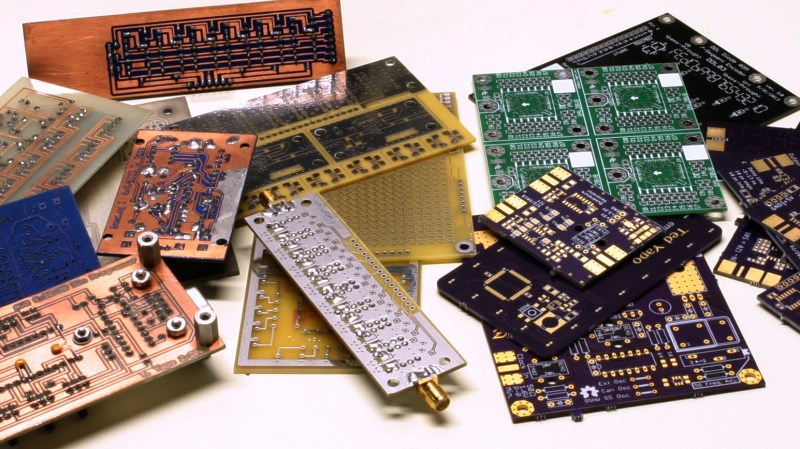
Many readers are certainly familiar with the process for home-etching of PCBs: it’s considered very straightforward, if a little involved, today. This was not the case in my youth, when I first acquired an interest in electronics. At that time, etching even single-sided boards was for “advanced” hobbyists. By the time I started etching my own PCBs, the advanced hobbyists were on to double-sided home-etched boards — the only type not pictured above, because I couldn’t find the one successful example I ever created. I later saw the rise of “bare bones” fabricated PCBs: professionally made fixed size boards with plated-through holes, but no soldermask or silkscreen. Eventually, this gave way to the aggregating PCB services we have now with full two-layer boards, complete with soldermask and silkscreen.
Today, the “advanced” hobbyist may be using four-layer boards, although the four-layer adoption rate is still relatively low – OSH Park produces around 90% two-layer and 10% four-layer, for instance. I think this will inevitably increase, as has been the case with all the previous technologies: the advanced eventually becomes the mainstream. Each of the previous shifts has brought easier design and construction as well as improved performance, and the same will be true as four layers becomes more commonplace.
So, let’s take a look at designing four-layer PCBs. If you’ve never considered one for any of your designs, you may be pleasantly surprised at what little extra cost is involved for all the benefits you gain.
How Do They Stack Up?
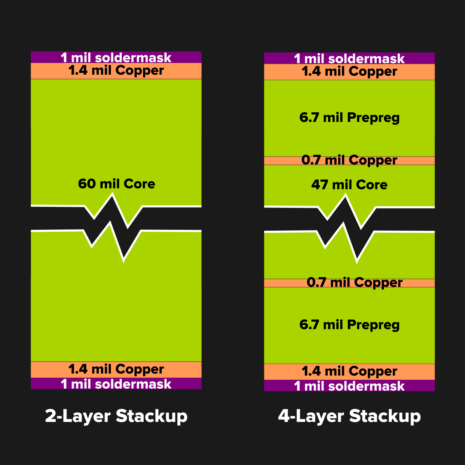
The obvious difference between two-layer and four-layer PCBs is two extra layers of copper. The particular arrangement of the layers within a board is known as a “stackup.” Two-layer stackups are simple: there’s copper of a specified thickness on each side of a core material, most often FR4 glass-reinforced epoxy laminate. A typical example is shown in the figure: 1.4 mil (aka 1 oz) for the copper and 60 mils for the core. If you’ve never worked with four-layer PCBs before, you might assume the extra two inner copper layers were equally spaced within, but they’re typically much closer to the outer layers. There are some very compelling reasons to do this, which we’ll explore in a bit.
If you’re ordering a large number of PCBs directly from the manufacturer, you can customize the stackup, changing the spacing and copper thicknesses to suit your design. With hobbyist-oriented services, however, you get their standard four-layer stackup. Luckily, many services have chosen their offerings well. OSH Park, for instance, uses a premium FR408 substrate for their four-layer service, which yields excellent RF performance.
What Goes Where?
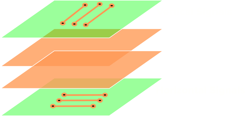 So, now you’ve got two more copper layers – what should you do with them? There are a number of ways to arrange your design, but unless you have specific reasons, it’s best to stick with the most common strategy. In this approach, the outer layers are used for signals, and the two inner layers are used as power and ground planes. Most commonly, the ground plane is closest to the component side of the PCB. Signals are then placed on the two outer layers. One convenient way to do this is to route signals in orthogonal directions on the two layers – the top layer might have primarily vertical traces, while those on the bottom would be mostly horizontal. To get to somewhere on a diagonal, you take a Manhattan-distance path, alternating between layers. This increases the achievable signal density, and is a good starting point for iterating on a design.
Connections between the layers are made with vias, just like in two-layer stackups. To power an IC, for instance, the pin may be broken out with a short, wide trace to a via which connects to the power plane. Better yet, you can create a small “power island” made from a copper pour on the component side which is connected to the plane through several vias, adding one or more bypass capacitors nearby for rock-solid power supply. With multi-layer PCBs, there are different varieties of via, although in hobbyist-level offerings, you typically will be limited to the more familiar type that goes through all layers of the board. In more advanced board processes, you can also have blind vias which only connect outer layers to an inner layer, or buried vias which only connect inner layers.
Why Am I Doing This?
OK, you’ve chosen to go with a four-layer stackup and the standard layer arrangement. What does this buy you? First, power distribution is greatly simplified and improved. Nearly solid planes, broken only by vias, have very low inductance and resistance, improving power quality, plus there’s no need to fit wide power traces onto the signal layers. Anywhere you need VCC or GND, just drill down for it. Without power traces on the outer layers, there’s that much more room for signal traces.
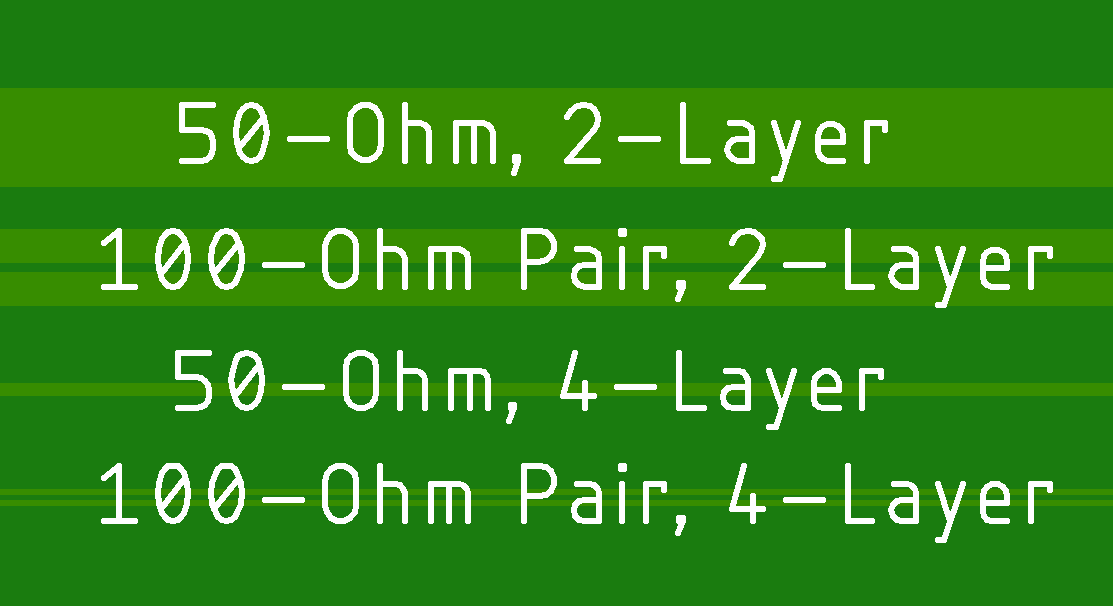
There are even more benefits for RF or high-speed digital designs. A 50-ohm trace on a typical two-layer board is around 110 mils wide. On the example four-layer stackup shown above, that drops to 14 mils, nearly a factor of eight improvement in density just from the track width. Differential digital signal pairs can also be improved, shrinking their footprint by a factor of four in this example. These advantages can easily result in more compact, yet easier-to-route designs, saving you board area and precious design time.
Some of the biggest pluses of moving to four-layers may not be immediately obvious, but there are more advantages to the small distance between the inner copper layers and their respective outer ones. Keeping the signal traces close to a power or ground plane increases the coupling between them, and decreases the signal loop area including the current return path. These factors decrease radiated emissions and improve signal integrity. If it’s just a hobby project, you may not be thinking of emissions testing, but if you ever want to get your design certified for sale, it can be a showstopper issue. Improved signal integrity, on the other hand, means you have a greater chance of a successful high-speed design the first time.
These advantages can be dramatic and almost come automatically. As a great example, Dave Jones over at eevblog recently posted a video where he took an existing two-layer design, the Gigatron TTL microcomputer, and changed it to four-layers simply by adding power and ground planes in between the existing signal layers. When he noise-tested the PCB, emissions from the four-layer version were greatly reduced compared to the original design.
Where’s The Catch?
So, that all sounds awesome, but surely there must be some disadvantages to four-layer designs. Yes, but they’re relatively minor. First, four-layer boards cost more than two-layer boards on a per-area basis. Typical numbers are from 1.5 x to 2 x the cost for boards of equal quality, not counting the really cheap “deals” on leaded HASL finish two-layer prototype-grade services. This metric can be a little misleading, however. A four-layer design may be smaller than the corresponding two-layer version, negating some of the per-area cost difference. The cost of the PCB may also be a small fraction of the total BOM, so doubling it will only add a small incremental cost.
For one-off and personal projects, using a four-layer stackup may pay for itself in the time and effort saved routing the design. If you’re planning a production run, four layers may still make sense, even if it’s just for a prototype that you can later try to cost-reduce into two-layers. Get it working quickly, then optimize later.
Another perceived disadvantage is the increased production time for the more complex four-layer process. This may have been more of an issue in the past, as the times are becoming more comparable lately. OSH Park, for instance, ships 90% of its two-layer orders in 8 calendar days, and an equivalent proportion of their four-layer ones in 9 days, with the times expected to equalize within the next few months. Combined with real-life shipping times, minor differences like this are completely inconsequential.
Besides time and cost, there may also be minor functional drawbacks to four-layer designs. Reworking a four-layer board to correct mistakes in a prototype can be more difficult than fixing a two-layer version. Since the inner layers are so close to the outer ones, it doesn’t take much extra force to accidentally cut into a ground or power plane when surgically disconnecting a signal trace. This can cause either side of the trace to short to the plane. A light touch and a thorough check with a microscope is advised. On the other hand, if you’ve routed signal traces on inner layers for some reason, re-working the board may be next to impossible: another reason to stick power planes in there.
Routing a four-layer PCB can involve some new twists, requiring a little extra thought. For instance, in the four-layer stackup described above, signals on the bottom layer are referenced to the power plane; their return current must flow through the plane to the nearest bypass capacitor to find its way back to ground. If you’re switching layers often with high-speed signals, you may need to add additional bypass capacitors between the planes at strategic points on the board to shorten these return paths and keep signal loop areas small. The upside is that doing so is simply a matter of placing the caps and dropping a few vias to connect them to the internal planes.
Finally, your favorite PCB layout tool may not support four-layer boards. Eagle’s free version is limited to two layers, as is Fritzing. If you use a hobbyist-oriented package, you’ll need to verify that it will do more layers. This may be the most compelling reason I’ve heard yet to get started with KiCAD.
Going Forward
Given all the advantages that four-layer designs bring and the minimal extra cost, it’s probably worthwhile to evaluate if any of your current or future designs would benefit from stepping up. Personally, I usually start with four-layer designs these days. About the only time I use two-layers is for extremely simple boards, or when I need them quickly, since I can get rush two-layer orders in about a week (coincidentally at the same price as normal turn-time four-layers).
There’s no reason to stop at four-layers, either. Similar arguments can be made for moving to higher-layer stackups. For a particularly interesting take, check out Kerry Scharfglass’s talk at last year’s Hackaday Superconference, where he describes spending an extra $130 to move his 500-piece order from four-layer to six-layer and saving an estimated 20-30 hours of design time.
You might be see a similar savings on your next project. Give it a try.
[Thanks to Laen and Drew at OSH Park for their insights and data.]


Not knowing what you meant by HASL, I looked it up Hot Air Solder Leveling.
https://www.7pcb.com/blog/enig-vs-hasl-different-surface-finish-techniques.php
And decades ago, I read about “Stripline” being used for RF circuits.
How does that fit in with multi-layer PCBs?
In the case of modern 4-layer PCB’s it’s just offset. Stripline is a signal line wedged between two ground planes, and most calculators assume it’s evenly spaced between the two (looking at kicad’s calculator, it doesn’t seem to do offset stripline) . I think there are a few offset stripline calculators that should show up on google.
As a starting point, I’d check out kicad’s TransLine calculator, it’s got good pictorials of various configurations. I like coplanar wave guides with ground plane personally.
Stripline may be easier in 6+ layer stackups where there are more chances for 3 evenly spaced layers, but even then that’s not necessarily guaranteed, as usually such stackups are (basically) layered sets of 1 and 2-sided PCB’s. In the case of the case of the 4 layer PCB above, think of it as two 6.7mil thick pre-preg boards sandwiched together on a 47mil core. As you start stacking 2 layer boards, at some point, the layer thicknesses between two prepreg boards isn’t necessarily guaranteed (unless you’re doing controlled impedance as an extra option, which costs $$). Disclaimer: I don’t know if they take two 2-layer boards and sandwich them together, or if they take a 2 layer 47-mil core and slap on a 6.7mil single sided board on each side. Doesn’t really matter for this particular case.
KiCad’s PCB calculator does handle asymmetric stripline — the trace-to-plane (‘a’ in the calculator) and plane-to-plane (‘H’ in the calculator) distances are specified separately. I was just using that a couple days ago, despite the fact that I’m still stuck on DipTrace for doing the board design.
On the fabrication side, the core is fabbed like a two-layer board, then uncured (i.e. still soft) prepreg layers are laminated on to it. This has the side effect of making the outer dielectric thickness somewhat variable, since the prepreg will distort and flow around the contours etched into the inner layer copper before it cures. Full, flat plane layers keep things nice and even. If you have any reason to care about slight variations in that thickness, though, you probably needed an uninterrupted plane layer for electromagnetic reasons anyway.
Stripe line has reference plane on both side (vs microstripe on one side i.e. signal on top or bottom layer)
Therefore stripeline requires to be in the inner layers of a multilayer PCB. Thinner traces is needed, but it’ll have more dielectric losses (at higher frequency).
What about capacitance between layers?
Is it anything to worry about? Is there an added benefit?
Between power & ground layer, it can help as very high frequency decoupling. However the separation is a bit far for the 62mil 4 layer PCB. Less separation (thinner boards or more layers) would help out.
PCB trace impedance is lowered by the proximity of a power or ground plane – less inductive because of smaller loop area, more capacitive . This reduces crosstalk between adjacent signal traces as the EM field like to concentrate more to the return path.
Spoiler: Up in the 20+layers, adding more layers won’t help routing as the vias starts to interfere with the routing. The PCB also starts to become thicker and more difficult to make.
That’s basically controlled-impedance layout, controlling the transmission line widths at frequencies or rise times high enough that you care about these effects.
The distributed capacitance doesn’t hurt, but it’s not high enough to replace proper capacitor use.
And it only costs 3X to make!
Did you read the article? The time saving, space saving, lower failure rate because fewer vias etc. can really make it worthwhile especially if you’re making production boards.
why not eight layer? cost maybe? :-) four layer is way easier to route, but I seldom can afford the extra cost of four layers,
I got a shipment from JLPCB yesterday. 10 boards 2 layers 100x100mm $2 + free shipping – yes, my PayPal says $2. Sent it on the 21st, got it on the 26th. The page says $56 a square meter! 4 layer 10 pieces is $29 + $8.60 shipping. 6 layer is $72. Stencils are $6. Better quality than my last from DirtyPCB’s. I had been avoiding designs with more than 2 layers. No more! I’m near Seattle, they are in Shenzhen. https://jlcpcb.com/
That is a “special offer”. I don’t know where my board house get their pcb’s from. Every penny saved is a penny earned. if the design does not warrant using 4 layer, i wont use it. my customers thank me for that.
I was telling Ted, when reviewing this article, I took apart a hand-soap dispenser only to find a single layer board, no mask, with two of those wire jumpers to cross signals, in something that was made in the last two years. There’s some volume at which these savings make sense.
But as a hobbyist, I would have to actively go looking for a one-layer no-mask board, and in single quantities it just wouldn’t be worth it.
When the price gap between two- and four-layer boards shrinks even just a bit more, the same will be true there. It just won’t be worth spending an extra hour on layout to save $5 on the PCBs in small quantities.
A product we made back in 2000 was a 4-layer board about the size of A5 paper. We’d costed it down to shrink the PCB area further, but were limited by the placement of connectors on the chassis.
We then worked with the (very large & well-known) customer’s inhouse cost-down team who chopped the 4-layer board right down to around 100mm2, added a bunch of single-layer pcbs at the connectors, and socketed interconnecting ribbon cables.
As relatively low-volume manufacturers ourselves, we were amazed how seemingly counter-intuitive changes resulted in a massive cost-saving.
>A four-layer design may be smaller than the corresponding two-layer version
Only if you are more aggressive in the placement and routing like a high end commercial product. Most OSH Park layouts aren’t.
That’s not necessarily true. Even with components only on one side, having power and ground planes on additional separate layers may allow for a smaller board size that just isn’t practical, or won’t even work, on two layers. Once you get to higher speeds and/or impedance-critical designs, power and/or ground planes may be the ONLY way of placing components closer together while allowing for lower-impedance power and ground paths and consistent signal line impedance.
When you start putting components on BOTH sides of the board, the above-mentioned restrictions become even more evident and harder to solve without a more-than-two-layer stackup. I’ve only designed one board like this, and to both meet the size restrictions and keep the DDS chip happy the ONLY way was a four-layer board with components top and bottom.
Eagle: tools/stats “packages used area” divided by total board area gives you an idea of utilization
My 2 layers PCB designs typically has around 65% area filled by single sided components. I got one populated on both sides at around 70%. I might be able to squeeze another 10%, so there is not much of board area savings.
Putting components on both sides means extra steps in assembly and cost more in production. It’ll be a pain for DIY oven reflow.
As much as I like to use multilayers PCB for a hobby, I can’t justify the cost and the extra import duty+ insane brokage fees as 4 layers pushes above the threshold. Yes, we have stupidly low import thresholds that sometimes I feel like I better off in a 3rd world country.
BTW we did 20+ layers at work, so I am well aware of signal integrity and the benefits/draw backs.
ExpressPCB.com does 4-layer boards (inner layers have to be planes, I think). Check ’em out. Free CAD tool, we use it for quickie stuff that we would previously have done with perf board and wire. Three boards will cost you something around $200, in 3 days.
3pcb and pcbway will do 10x 1000x100mm 4-layer boards for $50 with 4 day turnaround. Might want to stop throwing money away with expresspcb and check them out. For $200 you can get a 6 layer with 3mil/3mil traces
Well, I wouldn’t call ExpressPCB the cheapest, but it’s also not throwing money away. Big plus is their CAD tool is bare bones and free. This makes the learning curve short, and free is always nice. It’s not Allegro or Altium by any means, but it works and gets me boards quickly.
Thanks for the price point on those other two vendors. I’ll check them out!
Anybody making boards in small quantities should know about pcbshopper.com, which aggregates pricing for prototype PCB fabs. JLCPCB usually shows up on top (e.g. 4-layer, qty. 10, 100×100 mm for $30 + shipping, and they’ve started claiming controlled impedance) unless you’re doing something small enough that OSH Park’s per-square-inch pricing wins. I avoid ordering stencils from JLC, though, since they only offer one size (gigantic) and it jacks up the shipping cost.
For the last three designs I proto’d, JLCPCB was the cheapest and fastest by a wide margin.
10-20 boards, with 2 layers at 2oz, 10/10 spacing, and shipped in five days for $32.
The previous designer worked in ExpressPCB and was quoted more than $400 for the boards. I spent a few hours moving his schematics to Eagle, and quoted less for the work. I get that they let you work fast (and their package library is alright), but for simple designs, Eagle & KiCAD are not so daunting.
JLPCB also takes KiCAD gerber and extensions and drill files directly.
I’ll just add this about ExpressPCB: it’s the absolute quickest way for any of us to get a breadboard fast. We aren’t PCB layout people, we’re engineers who want a breadboard to test out a part, or interface to something or…well, whatever. We do have OrCAD and Allegro, but we don’t use them often enough to be good at them. ExpressPCB requires pretty much no learning time, and costs us nothing.
In the olden days, we would have pulled out the perf board and busbar, stuffed in the DIP packages and thru hole Rs and Cs, and built up our circuit. Two big problems with that nowadays: we always need a second one, and the thru hole parts are getting hard to find. Add that to the fact that we don’t have a tech to push the grunt work onto, and our time is pretty expensive, so we need to cut corners wherever we can.
Fine, you say, but what about the little SMD to through hole adapter boards? Have you priced those? PCB gives us the ability to build our own footprints. Not perfectly, but close enough. At the price point involved, one order ends up costing the same as a couple of hours of an EE’s time. And we can build in ground planes, connectors, alternative components, etc. So a quick turn PCB definitely beats more than one copy of a perf board, even if we could get the parts in DIP..
If you are doing a board layout for a proto run, might as well use the actual tool to capture what you have. Anything else you are wasting time ’cause you have to recapture the design on the proper tools and sit down with the layout person (I presume).
I usually spend a lot more time doing upfront design/simulations and it pays off well enough. Prototyping is only when you really need to derisk something not for fooling around. I finished a design (start to finish) and passed certification in 6 months while the “other guys” was spending the same amount of time in the lab prototyping/debugging and who know what.
regarding “What Goes Where?”
I’ve routed many PCB’s in my live of which many 4 layers and only a few with more. But never did I need to obey the “rules” of: Top-layer vertical lines, bottom-layer horizontal lines ?!?! Why is this even mentioned, that’s the way a really crappy autorouter “thinks”. If you want as many vias as possible then follow that rule. If you want to make a functional circuit, follow the schematic and use your common sense.
Layer directions made sense back in the through-hole days, where it didn’t really matter which side a track was on, but not so useful with SMD
I work in a PCB Fab house, and I also wonder why the simplest design boards rigidly follow the top-vertical-bottom-horizontal rule. It has absolutely no difference in most of the designs.
I was going to post this as well, and I’ve done plenty of 2, 4, 6, 8, and 10 layer designs, and I’ve never even thought of having preferred directions on a layer. It’s flat out idiotic.
Horizontal on one side and vertical on the other is actually bad advice if you want signal traces with a small loop area (low coupling, low noise, etc). Not inherently so, but any time you swap sides, you are swapping being reference from one power plane to another power plane. The better rule is pick a side and stick to it. If you want to avoid a sudden impedance change and a large loop area, you need to add decoupling capacitors between vcc and gnd near wherever you have signals switching sides. This allows the return current to switch to the other plane.
For most small designs, it won’t really matter. There will always be a capacitor nearby. But then horizontal on top, vertical on bottom won’t help your routing much on a small design anyway. If you go 4 layer, stick by the rule of trying to not swap layers, except near your start point or end point (since the return current will likely be going through a decoupling capacitor anyway).
https://blogs.mentor.com/hyperblog/blog/tag/reference-plane-change/
http://www.hottconsultants.com/techtips/pcb-stack-up-6.html
For a low noise/coupling 2 layer board, your ideal is a solid ground plane on bottom, and all signals on top. Your return path will always be on the ground plane. Of course there will be some breaks due to routing constraints, but just need to be aware of them and make sure any traces that route across such breaks are near the edge of the slot to reduce loop area.
I spent many years doing single-layer PCBs for volume products.
I still regard having to go to 4 layers as a sign of defeat!
I totally get that…
https://www.wired.com/story/coders-efficiency-is-beautiful/
Two layer to n-layer board conversion is trivial in the FOSS tool pcb-rnd, which has a drag and drop layer configuration tool. Want to move a layer? … drag and drop; want to add a layer? …. drag and drop.
https://archive.org/details/pcb-rnd-csect
pcb-rnd also loads eagle binary and XML layouts, as well as kicad layouts.
There’s one missing drawback of 4 layer board: soldering is significantly more difficult!
Even with proper thermal relief the two added copper planes absorb heat significantly and make soldering much harder, at least in my experience.
Should be entirely controllable by adjusting the size of your thermals. Never had an issue.
Might be good to mention capacitance per square inch, why Rogers materials exist, planar transformers, that energy is stored in spaces not in traces, single-sided PCBs and warping of large boards with uneven amounts of copper (hint, pour as much copper as possible), circuit “triplets”.
Very informative article . Will be using four layers the next time I’m designing a PCB because of it . Thanks
Ground planes kill one of my favorite techniques for prototype chip alignment :
Put the PCB on a back light (I often just use my phone
s torch). The total light transmission, through the pins, provides a very sensitive alignment methood.
I hope KiCad gets the same kind of makeover blender got. There’s just so many UI oddities, and I like Eagle way better despite it’s awful part creation system (Then again, the only part creation system I’ve actually liked is LibrePCB, and that’s still alpha quality although promising).
As for 4 layer in general, I don’t think I’ll be making many of them as hobby projects, but it’s fantastic to have an article on the advantages and cheese with them.
For hand soldering I try to do everything with 0805 and leaded packages, and I try to avoid surface mount mechanical parts, so my components take up way more space than routing anyway, but stuff still fits on a reasonably cheap OSHPark board.
In small QTY, where development time is more important than parts costs, my first step is usually to choose highly integrated components that don’t need as much fancy routing.
Hahaha, this article is a totally facepalm. I don’t know what’s the author development experience, but go by default to 4 layer PCB alleging enormous time saving is a CLEAR sign of lack of ablity. Even the more dense boards can be done with 2 layers, experience and some effort. You can requiere high power PCB’s or something special, but any else is act of cowardice.
Also is a lie the given price. 2x the 2 layer price?? Haha, maybe in eurocircuits or OSH, but they are expensive by default.
This image was mentioned, but not explained: https://hackaday.com/wp-content/uploads/2019/03/trace_comaprison.png. Can someone explain why the traces for a given impedance, as shown in this image, are so much wider for 2-layer boards? is it because of length? On a 2-layer board you have to route it a long ways so the trace must be wide to reduce impedance, but on a 4-layer board you just have a very short trace which then immediately goes to a via to connect to a power plane?
Distance between planes. Look up a formula for microstrip
I have done 4 layer prototypes with signals on the outside then moved the signals inside for production Inside a Navy Radio. EMI – difficult to find. About 40 years ago.