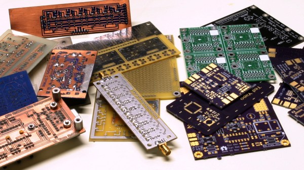
Many readers are certainly familiar with the process for home-etching of PCBs: it’s considered very straightforward, if a little involved, today. This was not the case in my youth, when I first acquired an interest in electronics. At that time, etching even single-sided boards was for “advanced” hobbyists. By the time I started etching my own PCBs, the advanced hobbyists were on to double-sided home-etched boards — the only type not pictured above, because I couldn’t find the one successful example I ever created. I later saw the rise of “bare bones” fabricated PCBs: professionally made fixed size boards with plated-through holes, but no soldermask or silkscreen. Eventually, this gave way to the aggregating PCB services we have now with full two-layer boards, complete with soldermask and silkscreen.
Today, the “advanced” hobbyist may be using four-layer boards, although the four-layer adoption rate is still relatively low – OSH Park produces around 90% two-layer and 10% four-layer, for instance. I think this will inevitably increase, as has been the case with all the previous technologies: the advanced eventually becomes the mainstream. Each of the previous shifts has brought easier design and construction as well as improved performance, and the same will be true as four layers becomes more commonplace.
So, let’s take a look at designing four-layer PCBs. If you’ve never considered one for any of your designs, you may be pleasantly surprised at what little extra cost is involved for all the benefits you gain. Continue reading “Stuck Designing Two-Layer PCBs? Give Four Layers A Try!”


