Back in 2016, Hackaday published a review of The National Museum of Computing, at Bletchley Park. It mentions among the fascinating array of computer artifacts on display a single box that could be found in the corner of a room alongside their Cray-1 supercomputer. This was a Transputer development system, and though its architecture is almost forgotten today there was a time when this British-developed microprocessor family had a real prospect of representing the future of computing. So what on earth was the Transputer, why was it special, and why don’t we have one on every desk in 2019?
![An Inmos RAMDAC (the 28-pin DIP) on the motherboard of a 1989 IBM PS/55. Darklanlan [CC BY 4.0]](https://hackaday.com/wp-content/uploads/2019/03/ibm_vga_90x8941_on_ps55.jpg)
This microprocessor family addressed the speed bottlenecks inherent to conventional processors of the day by being built from the ground up to be massively multiprocessor. A network of Transputer processors would share a web of serial interconnects arranged in a crosspoint formation, allowing multiple of them to connect with each other independently and without collisions. It was the first to feature such an architecture, and at the time was seen as the Next Big Thing. All computers were going to use Transputers by the end of the 1990s, so electronic engineering students were taught all about them and encountered them in their group projects. I remember my year of third-year EE class would split into groups, each of tasked with a part of a greater project that would communicate through the crosspoint switch at the heart of one of the Transputer systems, though my recollection is that none of the groups went so far as to get anything to work. Still how this machine was designed is fun to look back on in modern times. Let’s dig in!
Not Quite RISC
We were told as EE undergraduates that the architecture was RISC, but reading up on it nearly 30 years later I learn that, while it had a relatively simple instruction set, it achieved its one instruction per cycle not by RISC techniques but by clever use of a ROM microcode. Whether this was teaching by lies-for-the-children or the effect of Inmos’ marketing for the processor is unclear, but it’s certainly true that they were making a lot of noise about what the Transputer could do. I remember seeing the video below with its two-screen butterfly demo, ray tracing, and Mandelbrot set, and being bowled over by something that took my Commodore Amiga hours being performed in almost real-time by the Transputers. Yes, relatively low-definition ray-tracing of silver balls was a big deal back in the early 1990s.
The Transputer range was developed from an initial 16-bit offering in the early 1980s to a 32-bit version, then versions for SoCs including an ill-fated collaboration with Sinclair Research, and versions with inbuilt floating-point capabilities. The advantages of the Transputer architecture were eventually whittled away by advances in conventional processor performance, and by the early 1990s with SGS-Thomson in ownership of the company the Transputer development was halted. It had found its way into a range of niche products, but had somehow failed to break into the mass-market dominated by more conventional microprocessors from rivals such as Intel and Motorola.
Today both Inmos and the Transputer are footnotes in the history of computing. Oddly enough we are now surrounded by mass-market computers with multiprocessor architectures of British origin, but they feature the true-RISC ARM cores whose ancestors were in development at Acorn in Cambridge while the Transputer was grabbing the limelight. The Inmos semiconductor plant in South Wales is today owned by International Rectifier and is still in production, though its days producing Transputers are far behind it.
That Transputer development system at Bletchley is to be part of a restoration project giving the museum an exhibition of Inmos history. Meanwhile the Transputer itself may be dead, but it does have a descendant that is very much still in production. Xmos are another Bristol-based semiconductor company that specialise in CPUs for demanding audio applications, and since their founders include former key Inmos employees their cores are heavily influenced by the Transputer. I may never have encountered a Transputer after leaving university, but a quarter century later as part of a contract working on a high-end audio product, I came as close as it’s possible to get to one because it had an Xmos CPU.
The Transputer then, a bold vision of a semiconductor future that eventually happened, but not quite in the way that its creators hoped. If you find one, hang on to it, it’s a real piece of history!
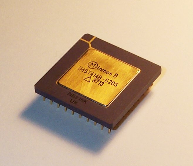
[Main image source: Inmos IMST425 by Konstantin Lanzet CC-BY 3.0]


We have some equipment at work that, if you watch the boot sequence scrolling past says “initialising transputers”. So there are still some, somewhere, doing their job.
https://en.wikipedia.org/wiki/Atari_Transputer_Workstation
The Atari Mega ST I/O board is like how Sony reused the PlayStation 1 core/system as a I/O processor for the PlayStation 2.
Not exactly the same thing but The Sega Genesis/Mega Drive essentially contained a Master System where the Z80 was used as a music processor.
meybe today Sony using Cell for sound and graphics/phisic coprocesor too?
Intel QPI is not unlike the interlink between the transputers. Yeah, it’s 20 serial lanes in parallel, but that’s just an efficiency improvement. With the higher end chips, they have 3 or possible more QPI links to enable a topology like the one shown in the video.
What’s the big steel shaft sticking out in the upper right of the transputer motherboard photo? Looks like the output shaft of a lawnmower engine.
Smokestack
Looks like it’s a screw boss. It’s threaded, if you look close.
Looks like the wrist pin.
I remember when they came out and there was some real interest in the Forth community. However, when we saw that for some reason they made the internal stack too short for the optimal algorithms developed by HP, people lost interest. I mean it something like 2 deep instead of 4.
But if they need Transputer systems at the museum, I happen to have an Archipel Volvox Supercomputer. http://www.regnirps.com/VolvoxStuff/Volvox.html
“I remember when they came out and there was some real interest in the Forth community.”
Apparently Harris didn’t work out.
No, Harris was all Phil Coopman, who had his own ideas on how things should be done.
Wow, with a Power Indigo 2 on top. Now the R8000 was also a bizarre CPU: the Cray killer. (Of course, SGI did kill Cray, by buying it. But that’s another story!)
I was working for SGI at the time that came out, right at the start of my career. Best support call ever: myself (support engineer), customer on the line, and the engineers who designed the PM (Processor Module).
Customer: “There’s a smell now.”
Me: “What?”
Customer: “There’s a weird smell now.”
Engineering: “Can you describe the smell.”
Customer: “Burning. Now there is smoke coming out.”
Long pause, silence on the line.
Customer (sounding panicked): “Um, guys, is this normal, or should I turn it off?”
Engineering, totally deadpan: “Yeah to both.”
The problem was that they’d put some non-conductive fibrous sheet (read: expensive insulating paper) between the heatsink and the PCB, and it was smarting to smoulder. But that was SGI for you: always releasing systems about six months early. As the COO used to say: “throw it over the wall and let support get it working!”
Don’t suppose that linux or BSD could be tun on it?
In the early ’90’s I worked for a start-up called Data-Cache. The product was to be a parallel-processing database transaction processing system using an array of Transputer modules. Each module contained a T800 Transputer, memory, and a pair of disk drives. The concept was that the database would be distributed across the array of modules, and processing of transactions would occur in parallel across all segments. Prototypes of the system were turning in very impressive transaction processing benchmarks. The base system we put together had 100 modules, with 200 disk drives, in three racks, linked in a toroid array. It was a total geek light show to see a transaction command enter at one node, and watch the activity wash over the array. Eventually, the proposed T8000 processor never appeared, the funding ran out (long story), and the software was purchased by Hitachi, where the idea apparently died.
I worked for a database company that was eventually bought by Sun/Oracle. It used arrays of 1U conventional Linux machines each with a couple of hard disks. The focus was on ultra high availability and reliability (at least 5 sigma) through redundancy and self repair rather than high performance, although it was fast. So, such architectures work really well even without Transputers. Also, a long time ago, ICL worked on associative memory to speed up search. Maybe, as Moores Law reaches its limit, the future will be about Transputer like machines where the emphasis is on hugely interconnected nodes rather than sheer increase in CPU power. A more brain like architecture. It may turn out that Transputers were just too far ahead of their time.
5 years ago I bought an xmos dev kit for testing purpose. Very interesting MCU with multicores with interlink communication. The xtimeCompser IDE was free to download. The langage used called xC is very interresting too. it is specifically design for concurrent programming using ‘interface’ concept similar to what is found in Go language.
xC is very interesting, and is essentially a modern version of Occam, the language for the Transputer.
xC and Occam are embodiments of Tony Hoare’s Communicating Sequential Processes (CSP).
Go and some other new languages have reused some of the concepts in CSP.
I like the XMOS devices, but think they are limiting themselves to the application spaces that they are currently targeting. Also, they could put more embedded memory on the devices. Otherwise, the XMOS devices could address numerous application areas that would fit between FPGA’s and microcontrollers (I’d take an XMOS device over a beagle bone for a few realtime I/O applications).
As a former Transputer programmer, I was initially happy to see the Xmos offerings but realized that they are more like ASICS rather than general purpose microcontrollers.
If you aren’t a professional developing the next Alexa you can safely ignore Xmos’s offerings because they don’t cater to hobbyists or experimenters. They used to but they evidently have stopped catering to anyone but monied professionals. The tools are complex and time consuming to master.
It’s not anything like the Transputer which was very easy to code for in Occam-2 and Parallel C.
BTW they are playing fast and lose with definitions: Their “cores” are really tasks. So if you’re thinking you’re getting a 16 core monster, you are probably getting a two core that can handle 8 tasks per core.
Xcore as part of a potentially new Amiga.
https://www.theregister.co.uk/2010/06/21/amiga_x1000/
The 16-core and 64-core Epiphany RISC OSC chips from Parallella are the closest modern chips to the Transputer chips that I know of. I have two of their 16-core boards which also has an FPGA Zynq 7020 chip with a hard ARM processor, https://www.parallella.org/board.
Introduction specs from page 10 of http://adapteva.com/docs/epiphany_arch_ref.pdf:
“The Epiphany architecture defines a multicore, scalable, shared-memory, parallel computing fabric. It consists of a 2D array of compute nodes connected by a low-latency mesh network-on-chip. Figure 1 shows an implementation of the architecture, highlighting the key components:
* A superscalar, floating-point RISC CPU in each mesh node that can execute two floating point operations and a 64-bit memory load operation on every clock cycle.
* Local memory in each mesh node that provides 32 Bytes/cycle of sustained bandwidth and is part of a distributed, shared memory system.
* Multicore communication infrastructure in each node that includes a network interface, a multi-channel DMA engine, multicore address decoder, and network-monitor.
* A 2D mesh network that supports on-chip node-to-node communication latencies in nanoseconds, with zero start up overhead.”
It’s unfortunate that Adapteva, the makers of the Parallela card with the Epiphany N-Core chip, seems to have shut down production and never managed to build their 1024 core version of the Epiphany {https://arxiv.org/pdf/1610.01832.pdf} with 1 MiB per core as that would be an acceptable minimum amount of RAM per core that I need for my new parallel object oriented language.
This type of Epiphany NK-core design, where N is 1 to a larger number and K is 1024, is the future, and in many ways is the Transputer/Epiphany connected cores approach catching up with current GPU offerings that have many thousands of much less capable and less general purpose GPU cores. From the GPU core perspective they are moving to be more general purpose overtime, maybe they’ll meet over time, however given the advantages of open source cpu cores Risc-V is a clear choice for massive NK-core connected designs.
Given that specialty computing cores such as the Transputer, Epiphany, and closed access GPU cores keep going out of production or have limited access to their internal architectures to address the need to be directly on the bare metal the future of these types of specialty NK-core connected designs will be dominated by the open source Risc-V designs. Take a Risc-V core and put 1024 of them on a single FPGA or ASIC chip (or as many as possible) and adopt the Epiphany connected network architecture (maybe Parallella will open that up, let’s ask Andreas Olofsson to do that).
Risc-V in a Transputer or Epiphany connected node configuration for FPGAs enables this form of parallel connected core computing to thrive independent of the market success or failures of any given processor company, and provides a path to ASIC for more massive numbers of cores per chip.
The internal network of the Epiphany design is impressive, from a software point of view the assembly language instructions can access the memory of any other node, the requests are sent over the node connected network with one cycle of delay per node connection distance. This makes writing software far easier for these parallel connected cores.
The external data connections of the Epiphany chips enables the chips themselves to be connected to four other chips expanding the mesh network of chips. Take four 1024-core chips and hook them up and boom, that’s 4096 cores each with massive IO capabilities as well. The software just needs to know configuration information to access all these cores. This approach allows as many cores that can be fit into a given FPGA to be connected up with multiple FPGA chips based upon the need and the economics of the products being made with them.
On a bright note it is very interesting that Adapteva’s/Parallella’s Andreas Olofsson has moved on to DARPA, https://www.darpa.mil/staff/mr-andreas-olofsson, to support “intelligent design automation, system optimization, and open hardware” at universities and industry. Olofsson is a supporter of Risc-V and related projects. He has stated that he has adopted Risc-V for the Epiphany chip, but I’ve not heard of any actual chips being produced with that modifed Epiphany design yet (the 16-core and 64-core Epiphany chips have their own Risc instruction set, Risc-V would likely replace that or enhance that).
Risc-V cpu core makers that seize the advantages of Transputer and Epiphany connected core designs will be able to scale to GPU scale core sizes in the thousands of cores and have an open source competitive solution to best proprietary GPU designs. A major advantage of the this design over the GPU cores is that each of these cores is a full independent CPU whereas the GPU cores are stripped down cores that have to operate in lock step with each other which is a huge limitation to running massively parallel general purpose computing software where each core is operating independently yet communicating over the fast node networks and directly sharing memory of the other compute nodes.
did you look at GreenArrays GA144 . A 2D matrix of computers, each one has its own memory and I/O. The CPU are stack machines, no FP.
“Take a Risc-V core and put 1024 of them on a single FPGA or ASIC chip (or as many as possible) and adopt the Epiphany connected network architecture…” Jan Gray has done just that on FPGAs, with his own ultralight network on chip. http://fpga.org/grvi-phalanx/
http://people.cs.bris.ac.uk/~dave/transputer.htmlhe pdf`s and as dave about making a new transputer inspired Risc-V cpu multi-core and The SURE Architecture – long version intigrated http://people.cs.bris.ac.uk/~dave/index.html
dave`s as disilusioned as us as regards mainstream vendors for a long time hence his law.
May’s Law states, in reference to Moore’s Law:
“Software efficiency halves every 18 months, compensating Moore’s Law.”
if the new Risc-V cpu core makers listen and co-operated and collaborated with dave and the remaining uk inmos guys then they could have access to the real deal
transputer floss derivatives for every diy maker to put into arduino to server cpb`s
opps see the pdfs at http://people.cs.bris.ac.uk/~dave/transputer.html
The central idea, multiple cores instead of faster clock speeds, has once again become popular. Looking at their demo, they may have essentially built the first graphics card, to boot.
“they may have essentially built the first graphics card, to boot.”
The Raspi boot from its GPU.
‘to boot’ is an idiom which means ‘as well’ in this context. ;-)
But that’s interesting that the Raspi boots from it’s GPU!
jacques1956, they did, and in fact the conections you never hear about is ibm gave them all their pattents as they where after the inmos sram etc
interesting fact about the SVGA standard, it was in fact the uk Inmos video RAM-DAC prototype for the transputer,and you can probably find data and perhaps code on that original test chip from dave may and the other uk inmos guru`s to re-implement its transputer essence here on esp32…
The FUTURE of Computing Performance
http://www.cs.man.ac.uk/CCS/res/res33.htm#c
Inmos and the Transputer (part 2)
Iann Barron …1982 …The story got worse. Eventually I had the ironic situation where I was in the US running the US company and I had to sell it off. It was actually sold to Seymour Cray, whom I had spent quite a long time trying to convince of the value of the transputer.
It wasn’t all doom and gloom because we had, as I have said, good technology. We had developed fundamental patents for static RAMs, for dynamic RAMs and for microprocessors, to the extent that every static RAM or dynamic RAM made involved a significant patent from Inmos. IBM was so concerned about our patent position in microprocessors they gave us rights to all their patents in return for rights in our patents.
Eventually dear old Thorn made something like £150 million to £200 million out of the Inmos patents, which is hardly ever mentioned. They got their money back all right.
There were two other money spinners. Our dynamic RAM technology was very good, and we were able to licence it to a Japanese company and set up an automated manufacturing facility in Japan. The other product was the second test chip we had made for the transputer. We persuaded IBM to use this as their next generation graphic chip, and it became embedded in the PC as the SVGA standard. Some of the oddities in the present Windows operating system stem directly from the way this chip was designed to work with the transputer….
May’s Law states, in reference to Moore’s Law:“Software efficiency halves every 18 months, compensating Moore’s Law.”
https://www.youtube.com/watch?v=8sO-jj9X2xc
Parallel Computing (Iann Barron) – Preparing for Parallella
Embecosm,Published on Aug 7, 2013
Iann Barron describing the history of parallel computing and its importance in the future of computing.
This talk was given as part of the Preparing for Parallella event hosted at Bletchley Park on 21st July 2013. https://www.youtube.com/redirect?q=http%3A%2F%2Fembecosm.com%2F2013%2F06%2F26%2Fpreparing-for-parallella-sunday-21st-july-2013-bletchley-uk%2F&redir_token=Eu0HJbyyaXWLzTLTRfTS51hVCR58MTU2NTExMjkwNkAxNTY1MDI2NTA2&event=video_description&v=8sO-jj9X2xc
https://www.analog.com/media/en/technical-documentation/obsolete-data-sheets/35026349641821151ADV476.pdf
Yes it has, although I don’t think they really had a choice. Not unless they wanted to stagnate.
https://www.anandtech.com/show/14211/intels-interconnected-future-chipslets-emib-foveros
I worked with the Transputer for about 6 years in the early 90’s and they were leaps and bounds above anything else at the time. It was a paradigm shift from anything before and after, that a lot of people just couldn’t get their heads around and thus dismissed as a outside niche product. The Transputer was heavily tied and co-designed with the Occam language and dislike of Occam, which once you get your head around it is very elegant. The Transputer was inherintly designed for parallel processing which no other processor I know of has been, everything else adds communications blocks and OS functions on top of the CPU. The big features were:
1) It was not CISC or RISC but MISC (Minimal Instruction Set Computer) which is stack based with as few instructions as possible. Using a stack instead of a register file (in CISC or RISC) means that instructions don’t have to include a two input and one output register locations. So while addition of (A + B = C) has to load A into a register, load B into a register, do the add operation that specifies the A and B and C locations and then store the C result back to memory. In a Transputer all you have to do is load A (always goes onto stack) load B (always goes on to stack), perform the add (which always sums the top two elements on the stack and then store (always from the top of the stack). So all the instructions were bytes, CISC and RISC instructions are 32+ bits today because they need to specify 3 registers do an ADD (two input registers and one output, assuming a 32 entry register file that is 3 5bit values or 15bits on top of actually needing to specify the operation. 8bits per instruction means that a single 32bit read for memory gets you 4 instead of 1 instruction, which means that Transputers didn’t need a cache and programs were 50% of less compared to architectures that used 32bit instructions. The draw back is that either you used a small stack and had to do more load/stores or used a bigger stack and had to do extra pops and pushes to get the data values into the top two locations. The Transputer went the small route and only had 3 stack elements so a total of 96 flip-flops was the entire register file and as mentioned before with no need for a cache the core was extremely small, mostly the 32bit ALU. Using 8bit instructions that didn’t have register addressing also meant that the 16b and 32b processors could run the same code or with only minor differences. Most of the Transputers had 4KB SRAM on chip so for limited applications they didn’t require external memory and this was much faster than getting data out of DRAM. Another benefit of all of this is that task switching between treads only required storing 3 registers (the stack) so task switching was a lot faster than any CISC or RISC.
2) As mentioned above the Transputer was co-developed with the Occam language and as such most operations in Occam compiled down to a single Transputer instruction including all the communications and task switching. Most people didn’t like Occam so immediately returned to C or FORTRAN (the two big languages of the day) but with out the inherent communications and task switching the writing of C or FORTRAN were much less efficient than Occam and imposed a 30-50% overhead.
3) Four on chip 20Mbit communications links so any processor couple send a message to 4 other processors. 20Mbit seems like not much, now but for the early 90’s when Ethernet was 10Mbit and very rare and most people were still moving data with floppies it was blazing fast!!! The Link hardware was part of the Transputer core not an external peripheral and the HW implemented the protocol so you just provided the message and sent it and the receiver would know the begining and end of the message and interrupt the receiving processor when a message showed up, not the arrival of a byte of depth of a fifo but the whole message whatever that might be, so no searching for headers or checking message lengths
4) Task switching and priority handling were also in-built to the processor there were two queues on high priority and the other low priority, they were at a fixed location in memory and you could have as many processes/treads as you wanted, a high priority process runs until it gets either to the end or needs to wait for resources (incoming message). Low priority processes would run either until complete or until then need to wait for communications or until a 64usec timer expired upon which the task would switch (all processors required a 5MHz clock from which a 15625Hz task switch clock was generated. So no OS was required the C and FORTRAN folks would usually add an OS but Occam was almost always bare metal, so no OS overhead but still had all the communications and task switching capabilities of a full OS.
5) Part of the Occam language was the CSP architecture (Communicating Sequential Processes) so part of the language was the allocation of processes to either a processor. The code for 10 treads on a processor was the same as one tread on each of 10 processors. Inter-process and Inter-processor communications were identical, the top level of code distributed the processors as you wanted. So a large applications could be fully developed and debugged on a single processor and then reconfigured to run more quickly on a processor array of 20 processors with a top level architecture file no other code changes would be required. As mentioned above the whole design of the Transputer was based on parallel processing so I was able to single handedly develop a 80 processor SONAR workstation in 9months, something that was impossible to even consider using the 386 processors of the time.
6) The whole processor array was connected with Transputer Links and a common 5MHz clock, reset and stop line. If an error was detected on any processor the whole array would stop, and a postmortem of any processor or process on any processor could be found which was a fantastic capbility that I can’t imagine on any modern development system and this was all automatic using the architecture file which specified each processor and process you could debug any value in the system without having to set anything up it was all automated withing the architecture.
There is more but I’ve already droned on, I think the Transputer was and still is light years ahead of anything else too bad it died due to corporate priorities, modern development systems could learn a lot from the Transputer architecture and the CSP concepts.
Once again this prove that it is not necessarily the best product that succeed on market.
Microsoft did a great job at killing off any of the OS competitors there were and most of them, except Microsoft, made heavy use of multi-threading and scaled to multi-processing quite easily. So trying to take a Microsoft developer into the threaded multi-processing world was quite painful. Distributed processing took a similar hit since it too was a threat to Microsoft so the effective implementations were attacked and only Microsofts weak DCOM survived for the short period after the collapse of things like CORBA. BTW, Netscape was attached because of one of the things it distributed was CORBA capabilities.
Things like Transputer and parallel processing were actively on Microsoft’s kill list in the 90s so survival was improbable.
Thank you very much for this detailed write-up of Transputer functionality.
I heard about the Transputer in the early 1980’s when I was 14 years old. I called up Inmos and figured out how to order a product brochure – they were quite confused why a 14 year old was requesting their product information – haha but I was obsessed with computers, already programming my Commodore 64 in assembly language. I wanted more power and the Transputer seemed like the future. I was enthralled by thinking about Transputer topology for most of my young school years, drawing networks and calculating network performance and optimizing the architecture – it was amazing tech for the time, no doubt.
I remember thinking up how to market a Transputer based computing system, including peripherals like printers that would have a Transputer chip inside, so if you bought a printer for your system it was also a CPU expansion due to the transputer inside the printer. Adding a hard drive would have a Transputer driving the disk, that could also be used as a computing node. Dedicated boxes stuffed with Transputer CPUs for more computing power. Instead of having to upgrade to a different faster computer, I’d just add more Transputers. I was so inspired by this chip.
I didn’t have money for a Transputer, so my dream of getting to work with them didn’t last – and I got an Amiga eventually, which captured my imagination and creativity.
I was thinking about the Transputer just last week, and wondered if it had progressed what kind of computing power it would bear – instead of 20 Mbit/s links, they would have 80 Gbit/s, instead of 4KB onboard RAM they would have megabytes of high-speed cache and gigabytes of local RAM.
Anyway, your comment was a fascinating read and I will no doubt come back to read it again because it was very detailed and enlightening to someone who always wished to know but didn’t quite make it that far with this unique technology.
I agree with neimad, you and badrectifier both wrote rather huge and lengthy comments but I read every bit of them and learned a lot never having heard of a transputer or the like! Thanks!
I remember reading about Transputers at the time and being particularly interested in the occam programming language. But once I learned about Amdahl’s Law, I became less interested.
With chiplets and interposers, CPU’s will probably circle back around to dedicated concurrent independent links between cores. But at the end of the day, they will still only excel at algorithms that can be parallelized. Since about 2005 clock rates have effectively stalled and are slowly starting to regress (ref: search for images of “42 years of microprocessor trend data” in your search engine of choice, or look at the graph of “chip frequency VS year of introduction” here https://hackaday.com/2015/09/09/exponential-growth-in-linear-time-the-end-of-moores-law/ ) effectively due to cooling requirements. Unless a more efficient refrigeration system is developed, maybe chips with builtin heat pipes, slower clock rates will be the future ( ref: http://slideplayer.com/slide/12890952/78/images/13/Power+Is+Another+Big+Problem%21%21.jpg ), we do not have enough cooling to switch/clock any faster.
We had a 50 node transputer system at uni for various assignments on parallel programming. They were programmed in some Pascal dialect. It was good fun, but the didn’t keep up with Moore’s race. The system was decommissioned not long after the student lab’s Sun workstations got faster on a single SPARC core.
In the late 80’s and early 90’s i worked on a large astronomy project – a plate scanner – and suggested the use of Transputers as we needed a significant amount of embedded computational power. You could easily build complex heterogenious computing structures in a lego like manner. We used pipes, work-farms, and star arrangements in our system. The final system had more than 30 T8 Transputers and ran 24/7/364 for over ten years.
I still consider the Transputer to be the best computing chip I have ever used as the designers of the chip really did know what their customers wanted – a solution that addressed both the software and the hardware for complex multiprocessor embedded systems. If they were available now I would use them without question.
If implemented in a present day silicon technology they would blow the competition away.
Oh happy days.
I believe TI dabbled in that design with their DSP chips in the early 90s. They used the multi-threading nature of OS/2 as the debug and development environment since there was so much going on in parallel.
Yes, I think their floating point DSP’s were heavily in this direction from the C3x, C4x, and particularly the C8x’s.
Yes the C40 was a faster C30 with 6 fast comm links much like the transputer. I first used one in about ’92. Each link had its own DMA engine, and you could do things like black hole routing between them ie zero CPU overhead passing a message from one link to another. I did a lot of C programming with them for sonar simulation. The C44 was similar but with 4 links not 6 I think.
Funny you mention using the C40 for sonar as that was the intended use at Scientific Atlanta back when I saw it.
Came here to mention the C30 and C40 families. I wound up doing a ton of work with the C30 flavors, always wanted to build something cool with those features only the 40 had, but economics got in the way. I wound up creating one of the first really good full duplex sound cards with the c31, (Musicad) while Creative was still fooling with half duplex 8 bit offset cards (the kewl kids were just getting 486’s then), and then using the same board (which booted from the ISA bus) later to develop the second implementation of VoIP to exist (after Ti/telogy which our consulting customer thought too shaky and too pricey). Great chips, make most others seem kinda less well designed and less fun to work with.
And then there’s Gustafson’s Law.
https://en.wikipedia.org/wiki/Gustafson's_law
Discussion of multi-threading.
https://forums.anandtech.com/threads/amds-hsa-when-the-same-on-cpus.2372542/
If there’s anyone out there who 1) enjoys hacking Makefiles, and 2) would like to help rejuvenate an embedded systems project, I’m one of the co-authors of the Transterpreter, which was a bytecode interpreter for the Transputer’s bytecode instruction set (ETC, or Extended Transputer Code). It was a virtual machine that runs on things as small as the 328p, and would absolutely sing on the current generation of ARM processors that we see on parts like the SAM21D/SAM51D.
https://concurrency.cc/
I’m just a college professor who doesn’t have as much time as I’d like for things like this, but if anyone is interested in helping me get the build system sorted out, it would be fun to bring this project back to life. It is a silly thing, but given that we’ve used it in the past for piloting UAVs, small robots, and environmental sensing… it’s just a riot to have a message-passing parallel programming language available for embedded systems development.
Or, not. But, I thought I’d chime in for anyone who wants to help keep a piece of computing history alive on modern hardware.
If you put the code up on github or gitlab it would be fun to take a poke at it.
I do a lot with 328 and small ARM stuff, and I read an Occam book 25 years ago.
The full repository, including the toolchain and everything else, is here:
https://github.com/concurrency/kroc
I have never mastered enough Make to get the cross-builds reliably working for embedded targets. It’s a large and old codebase, including the original INMOS compiler for occam, which was then extended to include extensions for memory allocation and mobility (occam-pi).
I’m happy to answer questions; we do have a mailing list, but it has been quiet for a few years. Feel free to drop me a note directly if you poke at this; I’m happy to join in.
Hi Matt,
I’m a bit busy with getting my own Transputer emulation system working (https://devzendo.github.io/parachute/) building on Windows, several Linuxes and macOS – but would be happy to try getting the Transterpreter system building on current OSs. I think I may be on your mailing list already…
Many thanks, Matt.
I suspect that the large platform builds are fine; anything with POSIX and GCC (plus any other languages in the chain…) should build cleanly. The cross-compiled embedded builds never fully got the love they deserved in the build system, however.
The mailing list is still alive… but very, very quiet.
I’ll reach out at some point. For me, having a parallel-safe language on the embedded platforms I’m working on is a big win. The TVM also provides multiple execution contexts, so it is possible to run multiple VMs on a multicore MCU, which is also a nice feature… you get safe message passing on small, multicore targets.
Time, as always, is the challenge.
Regardless, us maintainers of weird Transputer emulation/software implementations need to stick together. :)
Ah yes I remember spending a lot of time looking into using these – I was greatly disappointed.
* the stack was only 3 levels deep which meant the processor ended up doing a lot of unnecessary work. It’s like an ordinary processor (e.g. Z80, 6502) only having 1 index register that cannot be used with a displacement.
* the 4k on chip RAM was only accessible as words so you only had 2k words for the T212 or 1k words for the T414 / T800
* the “byte” wide opcodes required the use of special prefix opcodes. These took “real time” to execute. Loading a 32 bit constants (maybe an address) could require as many as 7 prefix opcodes – so 8 machine cycles to load a full 32 bit constant or address.
* the 3 register stack was ***NOT*** saved and restored on context switch. The transputer would automatically switch to an “alternate” task whenever it executed a jump (IIRC) opcode (there might have been other opcodes where it did this as well). During this special opcode execution the 3 register stack became undefined (you had to be careful not to use any of these special opcodes if you needed to preserve the contents of the stack). No context switch would ***EVER*** be performed until the special opcode was executed.
* when all 4 of the link engines were running at full speed the CPU would only run at 50% of its normal speed.
* the T800 used long sequences of opcodes to perform floating point math. These sequences were like setting up parameters to some microcode functions.
* there was ***NO*** interrupt pin only an event pin. IIRC the response to this was dependent on the scheduler.
You make some interesting arguments, but most do not apply to this design. You seem to be thinking in Intel mode. With parallel multiprocessing, One core can be dedicated to IO polling, eliminating the need for complex complex interrupt handlers.
Without the need for interrupt handlers, Context shifts are totally controlled by the running program, so results can be stored before shifting to another task. I have seen some newer designs using similar concepts (for example the Parallax Propeller”)
I designed a graphics board around the T800 that was used for chemical modelling, still have one in the loft. Also worked with Plessey ERA FPGAs – another British semiconductor company.
ST Microelectronics used a transputer core for their set top box chips until something like 2007. The first ten years of digital TV were DOMINATED by those chips. Started with ST20TP2 in around 1996 and moved through TP3 and 4 to the STi55xx series. The STi5512 was a very common chip in regular set top boxes for terrestrial and satellite while the STi5514 and 16 were very popular in PVRs. They had something like 3/4 of the market here at one point. Post 2000 NECs MIPS based EMMA1 and EMMA2 were the biggest rivals mainly for PVRs. My theory on this was that the transputer derived st20c2/c4 core was so tiny that more integrated chips were economically feasible before any other CPU, including ARM. This helped give STM a decade of shipping the most advanced chips first and most cheaply.
It did not survive the onset of high definition, which needed more horsepower. ST Micro tried to adapt but their new Hitachi CPU based designs lost to Broadcom’s MIPS and Connexant’s ARM SoCs.
Yes, the ST20 probably produced 1-2 orders of magnitude more fabs of the Transputer ISA than any chip marked Transputer.
BTW, NEC’s EMMA3 ended up in several HD-DVD players, cut short by Toshiba’s decision to stomp its feet and take it’s toys away, leaving NEC holding nothing. A bigger corporate temper tantrum was harder to imagine than Toshiba did that day. I actually forced Tosbiba to cough up the GPL2 code for the EMMA3 at one point, months later, due to my ownership of a HD-A1 player. I was really surprised they produced it, but I held them to the requirements of the GPL2, and a Taiyo Yuden CD-R dropped in my home mailbox with the code.
STM chips were so popular there were a lot of datasheet leaks. I think one Broadcom datasheet leaked early on. Neither EMMA1 or EMMA2 leaked a datasheet, it was like they barely existed. Might be just because they were unpopular. I owned products with them in but searches turned up nothing. EMMA1 had a trick I didn’t know about, one of the address pins, I think A9, had a (pull up or down, I forget) resistor on it, none of the others did. Made no sense. Turns out that configures the JTAG port on power up between boundary scan and EJTAG. Wish I’d known that at the time (>15 years ago). Someone a little smarter than myself and I reverse engineered the boundary scan chain and wrote a program to backup the firmware of an EMMA1 based device. I say EMMA1, there were two versions of EMMA1 and they had different chains, one was a STB chip the other a full but very early PVR chip. Early fond memories of just messing with hardware. Mostly getting going in circles but it was fun at the time.
EMMA3 I’ve never heard of before. Was the code bare of any driver stuff? That’s common for GPL releases from what I’ve heard.
I’ll need to find the CD. I requested the code in the weeks leading up to the HD-DVD consortium throwing in the towel, and it arrived months afterwards. By that time my interest had dissipated, and the HD-A1 containing it sits on top of a cupboard here (I wonder if it still even works – if it doesn’t I still have two XBOX360 HD-drives as well.)
The EMMA3 ASIC is well announced:
https://www.nec.com/en/global/techrep/journal/g07/n04/pdf/070404.pdf
https://tech.nikkeibp.co.jp/dm/english/NEWS_EN/20070124/126811/
It doesn’t seem like there was ever an EMMA4.
Please do find that CD. Host an image somewhere. It should not be lost to time.
It’s a shame it shipped with the absolute worst C compiler it’s ever been my displeasure to use, and that the peripherals were full of hardware bugs that weren’t acknowledged in the errata. By the time the alternatives became popular, I was begging for ST20 to die.
The debug hardware on chip for the ST20TP3 and onward was awesome though. Proper DMA memory accesses while the CPU is running, decent numbers of hardware code and memory breakpoints. Osprey was a little crashy on my system but considering ST20TP2 only had an OSLink for debug and you had to do RESET/ANALYSE like they did with transputers back in the stone age it’s like light came down from the heavens and dropped something perfectly formed in silicon.
I didn’t use the C compiler much and never had access to errata. I wrote much of my ST20 code in assembler but it was all amateur stuff. With better health I’d have done that as a job if I could. Now JTAG is locked out on anything like this (and often with serious cryptographic locks) and if I wanted to play I can’t. I miss the old era.
I suppose the downside to putting SO MUCH on a SoC is that errors creep in. The ST20 series needed a separate MPEG decoder IIRC. The STi55xx must have been insane to design, so many peripherals and an MPEG decoder.
Well there was also the ST20TP1, which was designed for the US market, having the necessary built in DES descrambler (the algorithm used to encrypt the packet payload data in the US), whereas the ST20TP2 was for the European market and had the DVB descrambler module. The TP2 was designed after the TP1, essentially a modification of the TP1 design. The well known (European) security standards of SECA, Nagravision, ViaAccess, Irdeto, Videoguard all use (or at least used to use, I have no idea if things have changed) the DVB algorithm.
The ST20TP3 followed the TP2 and had an upgraded CPU which incorporated instruction and data caches. I was shown a demo of two side by side Sky STBs, one of which was powered by the TP2 and the second by the TP3. Both responded to the same IR remote control. The TP3 STB was much more responsive than the TP2, such as the user interface and changing channels. It was a very eye opening demonstration.
Inmos was hardly *the* British semiconductor company. Ferranti, Plessey, Eliot, and ARM in its Acorn incarnation all did groundbreaking and globally significant work, to name but a few.
It’s mentioned in a comment above, but check out the GreenArrays GA144. http://www.greenarraychips.com/home/products/index.html
144 self-contained F18A computers on one chip, programmable in Forth. There’s TIS-100, a video game which uses this concept as well. http://www.zachtronics.com/tis-100/
Unless you’re a really good Forth programmer the GA chip is inaccessible to mere mortals. And you have to be really good at distributing the program across multiple Forth mcu’s with almost no memory.
In some ways it’s like going back to the early 80’s where you’re trying to make every byte count.
I looked into it almost a decade ago and saw it’s basically Chuck’s toy and not something industry will be adopting.
This GA144 is mainly memory limited, I have not seen a real application running on there. And nothing on their website http://www.greenarraychips.com/. To me it looks like a test chip that Chuck Moore – the inventor of Forth – designed for himself as a test, using the layout tools he wrote in Forth for GDSII. And it all worked. Unfortunately limited by die size at the time. There seems to be a new version on the way with more memory Greg has said. Fingers crossed, as I like Forth as a concept and a language, and published quite a few books about Forth. You can find them on amazon at https://www.amazon.co.uk/l/B00N8HVEZM?_encoding=UTF8&redirectedFromKindleDbs=true&rfkd=1&shoppingPortalEnabled=true as eBook or as print.
It’s kinda sad. I would buy one of these just to play with something interesting, but their “eval board” at $495 is ridiculously over-priced. Anything up to USD$150 can be an impulse buy, but over that it’s just not going to fly.
It’s really Moronic. With their millions they managed to kill the golden goose.
They have an advanced architecture, mentioned on their site for many years, but have never released it.
The price of the board and programming complexity killed sales penetration. It’s a common problem in some forth circles, to think something is easy.
They could have greatly simplified things with large address space support and memory bus and a few other buses and techniques, that didn’t require a lot of manipulation cycles to use. How many extra transistors does it take to have a core that can jump in a large address and step through it in execution. How many transistors does it take to have a shift register shift out data communications around and off the chip (using a delay for timing compatibility off chip) at higher speed, rather than bit banging? Waste. You want your core to be doing as much local work as condensed as possible when needed, minimising power and processing wastage of a lot of wake cycles.
The device may perform an instruction at very low energy, but it requires a lot of extra instructions to do things due to the lack of these advanced techniques, which limits it’s speed. Is it worth it?
Now, this new 18 chip with memory cores. Is that not what they talked about many years back? It is what should have been year 1 or 2. I hope for larger memories than the current addressing limits. This would enable buffering of work between cores with complex routines on them, allowing more cores to work more often on the work. This would give more flexibility in non streaming work flows, with tasks distributed around chip. Stuff which makes sense to many real world programmers. It is time for new blood there, for a long while.
Now, if you go to their ranch to design your stuff to progress the market (or whatever it is these days) take notice of who they claim owns the rights to your work there, or in any other business dealings you are paying.
Aren’t archetectures like these the basis of modern GPU design? The Transputer sounds a lot like CUDA cores/Stream Processors.
I think you’re correct. From Transputer to GPU to Neural Nets.
I’d like to hear more about the limitations of the transputer and why the concept of computational cells with links between them didn’t take off and petered out with the demise of the transputer.
Thanks for that detailed analysis.
I’d like to understand this at a higher level.
I understand that the transputers couldn’t be a good general purpose computer due to the considerations you mentioned.
Why do GPU’s with shared memory thrive today whereas transputers with highly optimized, limited number links fail?
Do you see an opportunity today for such a computer or for a resurgence of Occam?
This really brings back AI memories – those were the days of Parsytec and Manfred Helzle’s hema in Germany, see hema.de. I am sure there are still some transputers and transputer boards there – or even in FPGA.. And what was running as one application on such a multitransputer system? Nestor AI, NN, Adaptive Classification. The amount of transputers was not really limited – just cost. And this was about 30 years ago. We actually spent a week at Nestor in the US to get the transputer system running. I am quite surprised that there is no T-community as a 414 should be rather small and probably fits into an Arduino. The T-Links were not complex – just fast. Unfortunately like in other areas – Marketing wins, and not the best product – a similar story as the good old 1802, but here there are still a lot of followers with running systems – and I still own a few 1801s and 1802s. See http://www.cosmacelf.com/. Tom Pittmans comment at the time: “This microprocessor (1802) is so good that even RCA is not really aware of how good it is.”
Just came across a hema Transputer ISA board out of some recently retired semiconductor handling equipment!
In my experience the XMOS development tools are *very* easy to learn and use. I was productive within a day of starting development.
XMOS has, indeed, exited the hobbyist arena. I reckon there’s scope for someone to sell a board with one of their processors and a USB interface.
XMOS is *very* explicit about what their cores are and how they can be used. They are optimised for *hard* realtime embedded systems, hence the cores are in no way comparable to those in, say, x86 devices. But the latter would be useless for hard realtime embedded systems anyway.
Zerg, see my comment below starting “In my experience…”, which has become detached from your post.
Sigh.
Massively parallel hardware is trivial. What’s more difficult is the programming paradigm/language and development tools.
XMOS excels in the latter area, and the hardware/software integration is an impressive and useful achievement.
Well, Sega did use it to provide backwards compatibility for the Master System on the Genesis.
I swear i hit reply to djmips post and not reply in general.
I have actually used one of these during my studies. Our uni had a small development system with several nodes (each node was a plug-in card in a card cage) hosted on a Sun 3 workstation. We used Occam and PVM (MPI didn’t exist yet, I believe) on it. It was a fun system to learn on but fairly limited and pretty hard to debug because from the user’s point of view, the Transputer nodes were basically black boxes – if it locked up because you ran out of stack (the nodes had very little own memory!), for example, tough … It was more similar to embedded system development (just without JTAG!) than anything modern.
I had a colleague who worked together with the Paderborn University in Germany where they had a much larger Transputer machine on this, he has ported PovRAY on it.
Great article, and some great comments too. I worked at Inmos for rather a few years, including working on the glorious failure of the T9000. I’ve just posted about all this over on the retrocomputing forum: https://retrocomputingforum.com/latest
I have an old (1987) ISA bus card from a company called Nth Computing with a T800 and a T414. A rom chip is marked “Baby Ninja” . This board is paired with a memory expansion sidecard marked “AT 3D Display lists/Video expansion” .
I have never be able to find out any information about the board, and since many of the commenters have experience with transputer hardware, I am curious if anyone might know this board>
Gary, I also have in my possession a card with a chip marked “baby ninja”. However, I don’t know anything about it and right now it’s with a relative. For some reason I remember concluding that it was an early graphics card, so mine probably has the text “video expansion” as well. I’ll try and check the other details next time I get the chance.
The transputer was a standard part of the University of East Anglia’s Computer Science architecture module in the late 1980s. For my dissertation project, I implemented a imagine recognition Neural Net on our 9 node T424 transputer rack in Occam 2, which could be programmed from any terminal at the Uni.
CSP is undoubtably the best and easiest way to extract and apply parallelism in algorithms, but because it was considered too much of a hurdle to program non-sequentially in the 80s, we’re now stuck with over-engineered CPU designs that have terrible efficiency for concurrent operations using a plethora of ad-hoc hardware and software techniques.
The Inmos semiconductor plant in South Wales was taken over by Infineon in 2015 when it bought out International Rectifier, who then sold it on, and it now runs as a Foundary (but who knows for how much longer.)
Dabbled for quite some time with Transputers, using a Mac512 with a modified motherboard with a C011 to connect to the Transputers. Porting the OCCAM compiler over to the Mac and writing a device driver for the Mac the Transputers then became a RAM based disk drive for the Mac. This was lot of fun, later I passed on all the Transputer hardware (about six boards) on to guy who said he wanted to do project which never came to fly. But these days I seem to be too time constrained to be able to such projects, not even with real RISCs
The Transputer is a fascinating architecture, and several emulators exist, including my own open source emulator/toolchain project:
https://devzendo.github.io/parachute/
There’s still some work to do before it’s finished: I’m currently working on a port to Windows, but it builds easily on Mac OSX, Raspberry Pi and CentOS.
It’s an emulation of the T800, although the floating point instructions are yet to be started.
If you’re interested in emulation, Transputers and language development and would like to join in, I’d love to hear from you!
Sounds like you and Matt Jadud (above) should talk. I had no idea there were so many knowledgeable people about the Transputer on HaD. I was a kid when these things came out. I was fascinated. I still have the databooks and a few T800 lose in storage somewhere. I’ve always dreamed about whipping up a board to mess with them. Glad to see there’s still so many resources available to help revive that project.
Yes, I’ll see if I can get the Transterpreter building on the platforms my emulator builds on. I’d like to have an occam compiler available on the systems I’m targetting, rather than the DOS environment I currently use it from.
There are other emulation projects out there, notably Gavin Crate’s emulators at https://sites.google.com/site/transputeremulator/Home
There’s a wealth of information on the architecture, history and software at Mike Brüstle’s site at http://www.transputer.net/
I don’t know about the T9000 but all other transputers before it only had a single core and could only execute a single task at a time. The tasks behaved just like a cooperative multitasking system. There was no pre-emptive option and the fact that you needed a task to poll I/O would just eat into CPU cycles for no reason and cause possible real time deadlines to be missed. Interrupts may not be to everyone’s liking but when used correctly they can greatly reduces the burden on a processor due to polling (they also make reaction to real time events infinitely more predictable and precise).
The transputers switched tasks ***VERY*** frequently and they did this by switching on certain opcodes such as “jump”. To make a section of code execute in its entirety (without interruption by other tasks) required care ***BUT*** also meant responding to I/O on a polled basis could be greatly delayed. Furthermore, adding extra tasks at a future date could greatly affect response.
If you start talking in terms of splitting a “job” into several tasks and putting each task on a separate core such that they all truly execute in parallel then you need to take into account the overhead of passing data between them on a serial link. Don’t forget, each transputer could only directly communicate with its four neighbours. If they wanted to communicate with any other transputer then you had to build an extra routing layer under the data you were trying to pass and all the transputers between the source and destination would take a processing hit.
Yes you could build a pipeline with a transputer in each stage (have each stage do a small amount of processing on the data and pass it on) and get some very impressive number crunching benchmarks. But in terms of general purpose multi-threading as we see it today on an i7 or Ryzen 5 forget it.
I strongly believe the reason the transputer died was because it could not live up to the hype. The people that designed it knew this and moved to pastures green while the transputer was still a success on paper.
hmmm, replies are not being inserted where they are being posted… WordPress weirdness???
Exotic or at least different processors always generate consideration. I recall late (lamented by me) Byte Magazine – Hackaday of its time- having CPU technical overviews of alternative processors like Transputer, Rekursiv, and “proof by design” Viper. A wild and crazy printer project looked at using a Data flow image pipeline processor from NEC. Not long after ARM became commercial an Asynchronous ARM design also seemed promising -around the same time as the AT&T Hobbit and ShBoom.
Sure, in the days when it regularly published Steve Ciarcia’s column.
Once that stopped, Byte transitioned into a publication which didn’t acknowledge that there were computers which ran anything other than MS-DOS, with an occasional grudging and dismissive mention of MacOS. It failed to differentiate itself in any way, so when it eventually disappeared, nobody noticed or cared. That disappearance was inevitable, because there was really no value anymore in it existing.
When Ciarcia started Circuit Cellar he defintely cited Byte’s (post acquisition?) lack of interest in publication hands-on articles. I think his last Byte article series built an 8051 supercomputer- scalable ISA bus cards filled with 8051s running Mandlebrot fractals. Into the early 90s Byte did maintain a system evaluation lab (Rick Grehan director AFAIR) and also covered less mainstream stuff from the era like the Intel i860, Mac Clones, SCO Unix, VM/386, and tablet computers.
I was one of the designers of the Rekursiv. I spent time at a small outfit in Brighton which was trying to graft a Rekursiv onto a Transputer system which they thought they could make run Unix. Once I discovered the Transputer’s limitations (no interrupts, no MMU etc) I made a hasty exit.
Nice. AFAIR Rekursiv had separate chips for CPU and Memory Object Management and seemed initially targeted for management of factories. I can’t recall the Rekursiv software development environment(s) – Smalltalk, an Object LISP, C++, Prolog?
I’d love to hear more about the Rekursiv — I remember the Byte article, and the garbage collection scheme, but I never saw anything more about it.
What happened?
For any other Transputer nerds still lurking here, I found a couple of other resources that should be included in this discussion. A mostly complete FPGA implementation of a T42:
https://tu-dresden.de/ing/informatik/ti/vlsi/ressourcen/dateien/dateien_studium/dateien_lehstuhlseminar/vortraege_lehrstuhlseminar/lehrstuhlseminar_ss17/20170720_T42_Transputer-in-FPGA_DesignStatus_DeptSeminar-Presento_UM.pdf?lang=en
And another emulator:
https://sites.google.com/site/transputeremulator/
If anyone wants to dig deeper, this is the best place to start:
http://www.transputer.net/welcome.asp
Lastly, it looks like Transputers are still available on eBay. Roughly $40 delivered on eBay at the time of this posting.
the untold story everyone seems to conveniantly forget see how inmos effected todays svga and sram/dram
http://www.cs.man.ac.uk/CCS/res/res33.htm
…Inmos and the Transputer (part 2)
Iann Barron
I’d like to hear why the funding ran out for what sounds like a promising project. (long story?) And why Hitachi would let it die. Please do share.
i have a couple transputer boards i dumpster-dived from a small southern ohio college in the 1990s — i even got one to boot once with software downloaded from the early internet (in fact, i first saw the power of the web when i did an infoseek query of the term “transputer”)
The INMOS Transputer was also used in the SKY HD and SKY HD+ series of SKY STBs now they have switched to an ARM processor for the SKY-Q STB. (sorry for shouting).