
In the first part of this series, we took a look at a “toy” negative-differential-resistance circuit made from two ordinary transistors. Although this circuit allows experimentation with negative-resistance devices without the need to source rare parts, its performance is severely limited. This is not the case for actual tunnel diodes, which exploit quantum tunneling effects to create a negative differential resistance characteristic. While these two-terminal devices once ruled the fastest electronic designs, their use has fallen off dramatically with the rise of other technologies. As a result, the average electronics hacker probably has never encountered one. That ends today.
 Due to the efficiencies of the modern on-line marketplace, these rare beasts of the diode world are not completely unobtainable. Although new-production diodes are difficult for individuals to get their hands on, a wide range of surplus tunnel diodes can still be found on eBay for as little as $1 each in lots of ten. While you’d be better off with any number of modern technologies for new designs, exploring the properties of these odd devices can be an interesting learning experience.
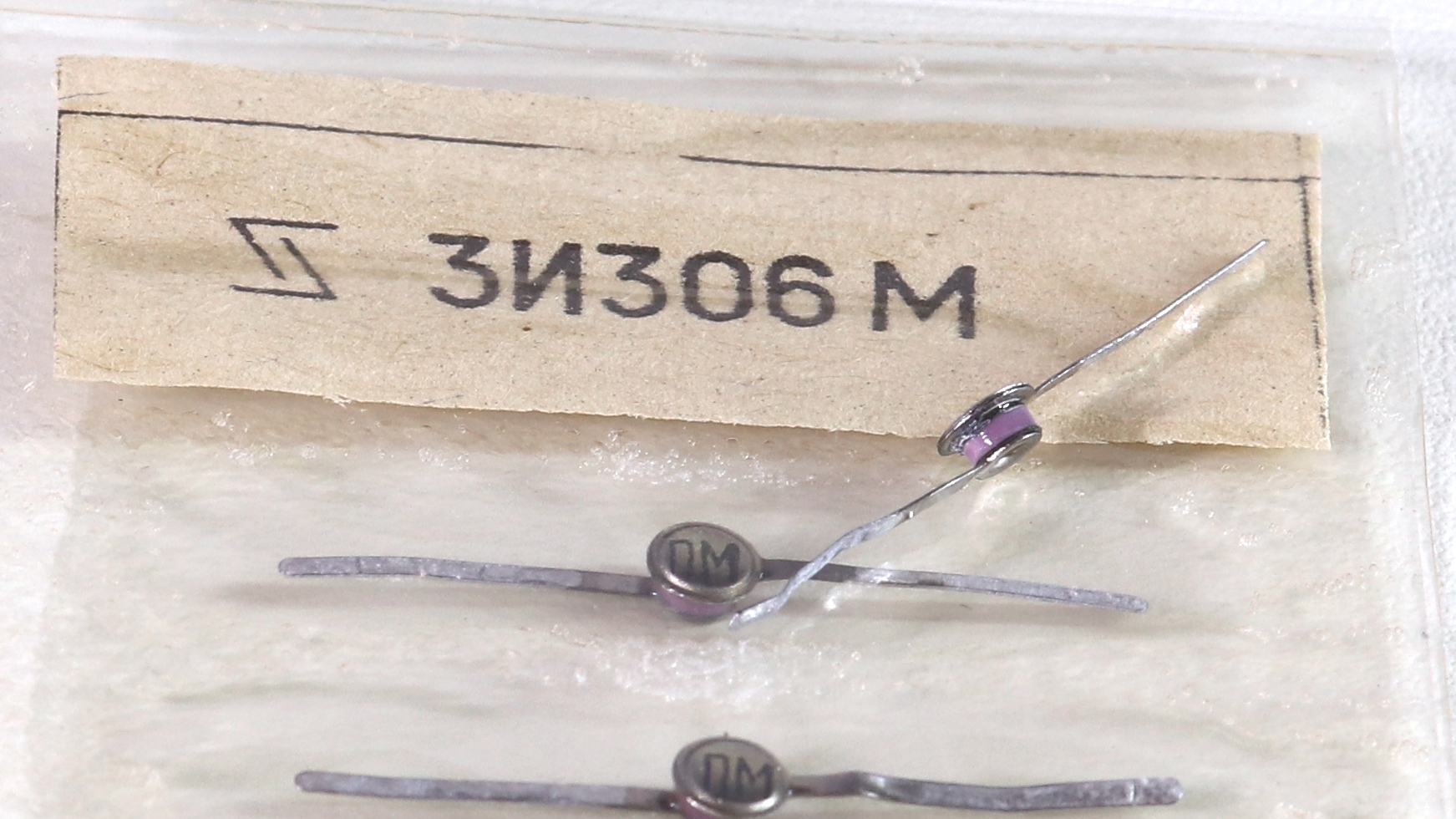
For this installment, I dug deep into my collection of semiconductor exotica for some Russian 3И306M gallium arsenide tunnel diodes that I purchased a few years ago. Let’s have a look at what you can do with just a diode — if it’s the right kind, that is.
[Note: the images are all small in the article; click them to get a full-sized version]
3И306M Tunnel Diodes
 I bought a set of ten of these military-grade gallium arsenide diodes in 2016 for some experiments with pulse generators. You may also see this part listed as “3I306M,” since the Cyrillic letter “И” corresponds to the English “I.” The TekWiki on w140.com has a good page on surplus Russian diodes, as well as good general information on tunnel diodes, especially those used in classic Tektronix oscilloscopes. Some diodes are optimized for use in amplifiers, pulse generators, or for switching circuits. From the 3И306M datasheet (PDF, in Russian), we can glean some information about this particular diode — a switching type — but I found it easier just to measure some of the parameters firsthand using a curve tracer, which generates the I/V characteristic curve for the device.
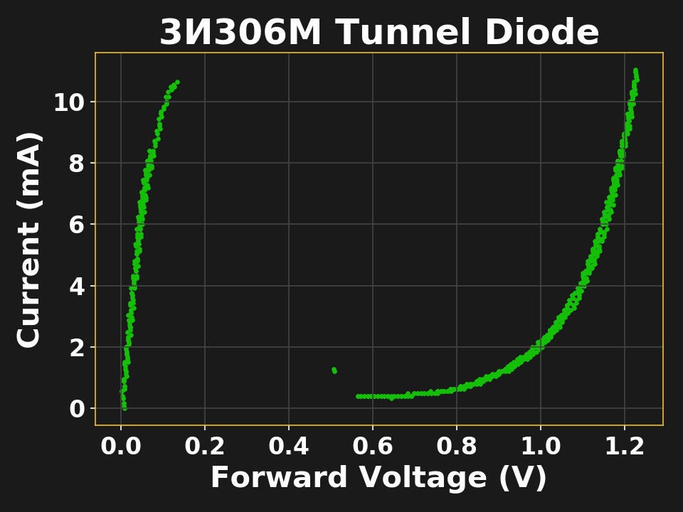
In the last article, I presented my quick-and-dirty curve tracer, which is nothing more than a signal generator, a 10-Ohm resistor, and an oscilloscope. I also mentioned the problem with that method: that the voltage measurement is corrupted by the current measurement on the scope’s screen. The ideal thing to do is capture the trace data and plot the curve in your favorite graphing software, where you can compensate for the error. This time, that’s exactly what I did, exporting the traces as a CSV file, then generating the plot in python using matplotlib.
As you can see in the curve, the current through the device initially ramps up to around 11 mA with increasing voltage until 150 mV, at which point the current drops abruptly to about 500 uA before increasing again. This is the negative differential resistance (NDR) region, where the current drops with increasing voltage. The interesting thing about this curve is that only two points in this region were captured. Looking at the waveform of the voltage measurement shows what’s going on — the diode is switching on and off at very high speed.
Switching Performance
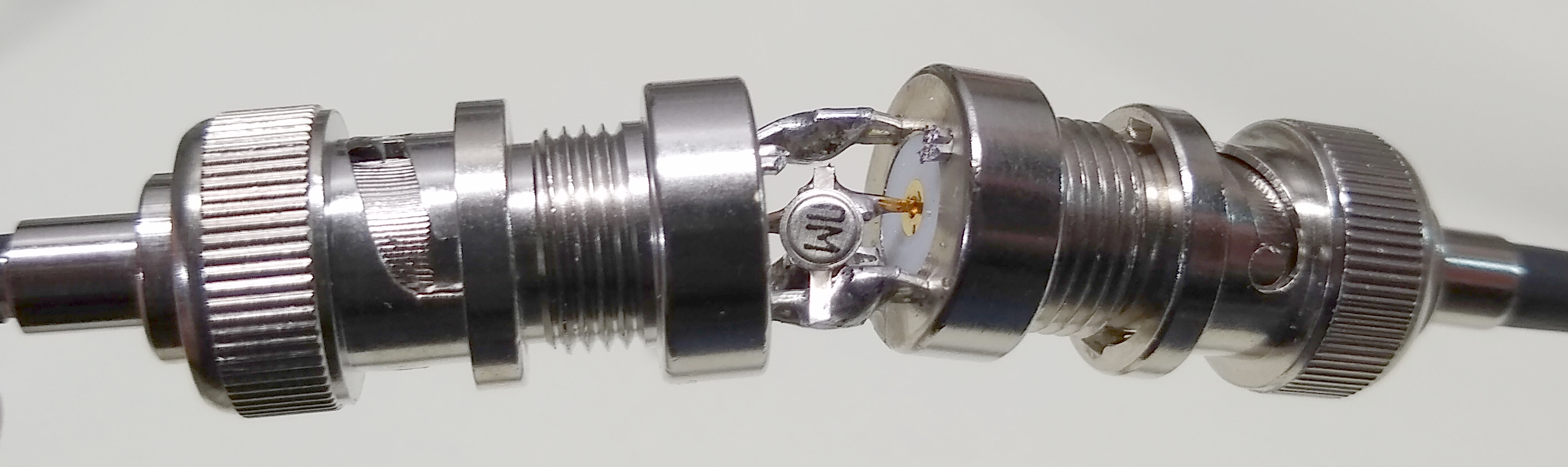
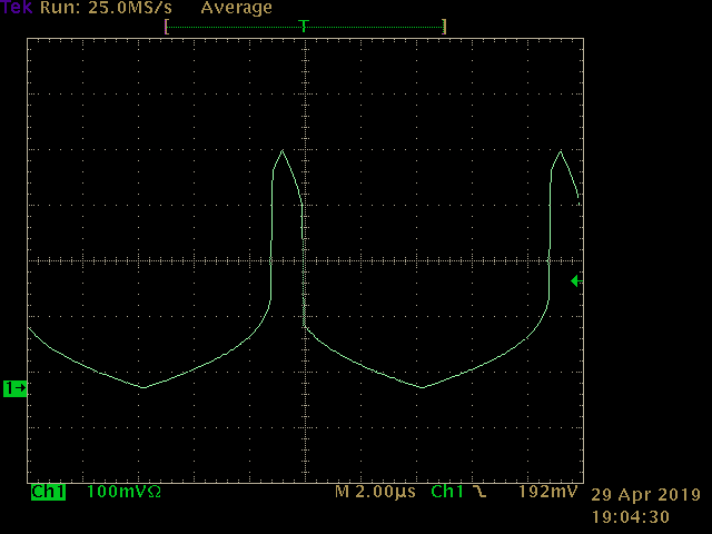
This diode was intended for switching, so it makes sense it should generate sharp edges. To get a better look at this, I built a test jig from two BNC jacks soldered closely together: the tunnel diode is soldered across the BNC terminals. With one end connected to a 50-Ohm signal generator and the other to a 50-Ohm terminated oscilloscope, this allows testing of the very fast switching speed of the diode.

The switching time of the diode seems independent of the input waveform — when the voltage hits the threshold, the diode switches — so I drove it with a triangle waveform at around 100 kHz. I measured the fall time of the output transitions at under 900 ps, while the rise time was slightly longer at 1.1 ns. That’s pretty impressive for a circuit with only one part (ignoring the signal generator). This could be just the ticket for sharpening up the lazy 100 ns edges on a classic 555 oscillator, if you were into that kind of thing.
The drawback to this circuit, common to all tunnel diode applications, is the low output level: these diodes work at low voltages and currents, so can’t generate powerful outputs.
300 MHz Oscillator
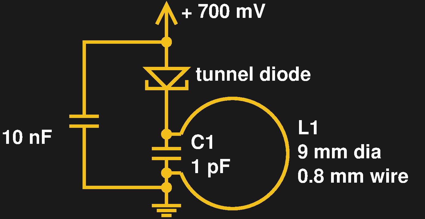
While this particular diode may have been intended for switching, it can easily be pressed into oscillator service. Like I did with the transistor circuit in Part I, I built an LC oscillator using this diode as the active element. The negative resistance of the tunnel diode counteracts the positive resistance in the LC tank, causing oscillations to build over time instead of diminishing.
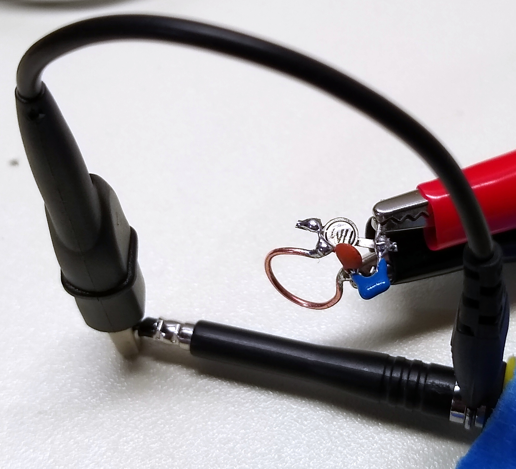
The resonator initially consisted of a single 9 mm loop of copper wire in parallel with a 2 pF capacitor – or so I thought. A 10 nF bypass capacitor handles the return current through the diode, and a 700 mV supply powers the oscillator, although I found that the circuit would continue to oscillate down to 330 mV once started.
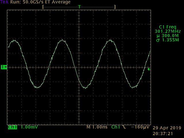
This circuit initially oscillated at 295 MHz. When I swapped the 2 pF capacitor for a 1 pF part, and the frequency only went up to 300 MHz, I realized that the capacitance of the diode itself was keeping the frequency low. By calculating the inductance of the wire loop, I was able to estimate the diode capacitance at around 18 pF (the datasheet only says less than 30 pF). This diode capacitance adds to the LC tank capacitance, reducing the resonant frequency.
For the same reason, care must be taken when probing a circuit like this. My 10x oscilloscope probe claims to have a 10 pF nominal capacitance, which would have a similar frequency-reducing effect if the circuit were probed directly. Instead, I attached the ground clip to the probe’s tip, forming an inductive pickup loop. Keeping the two loops close together acts like a transformer and gives enough coupling to detect the signal and measure the frequency. Since the coupling is somewhat arbitrary, the amplitude scaling is not calibrated, but changes to the circuit operation — due to changing the power supply for instance — can still be seen.
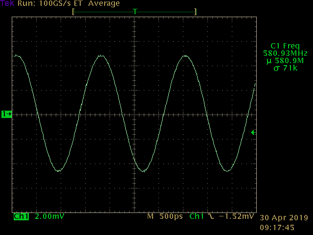
581 MHz Oscillator
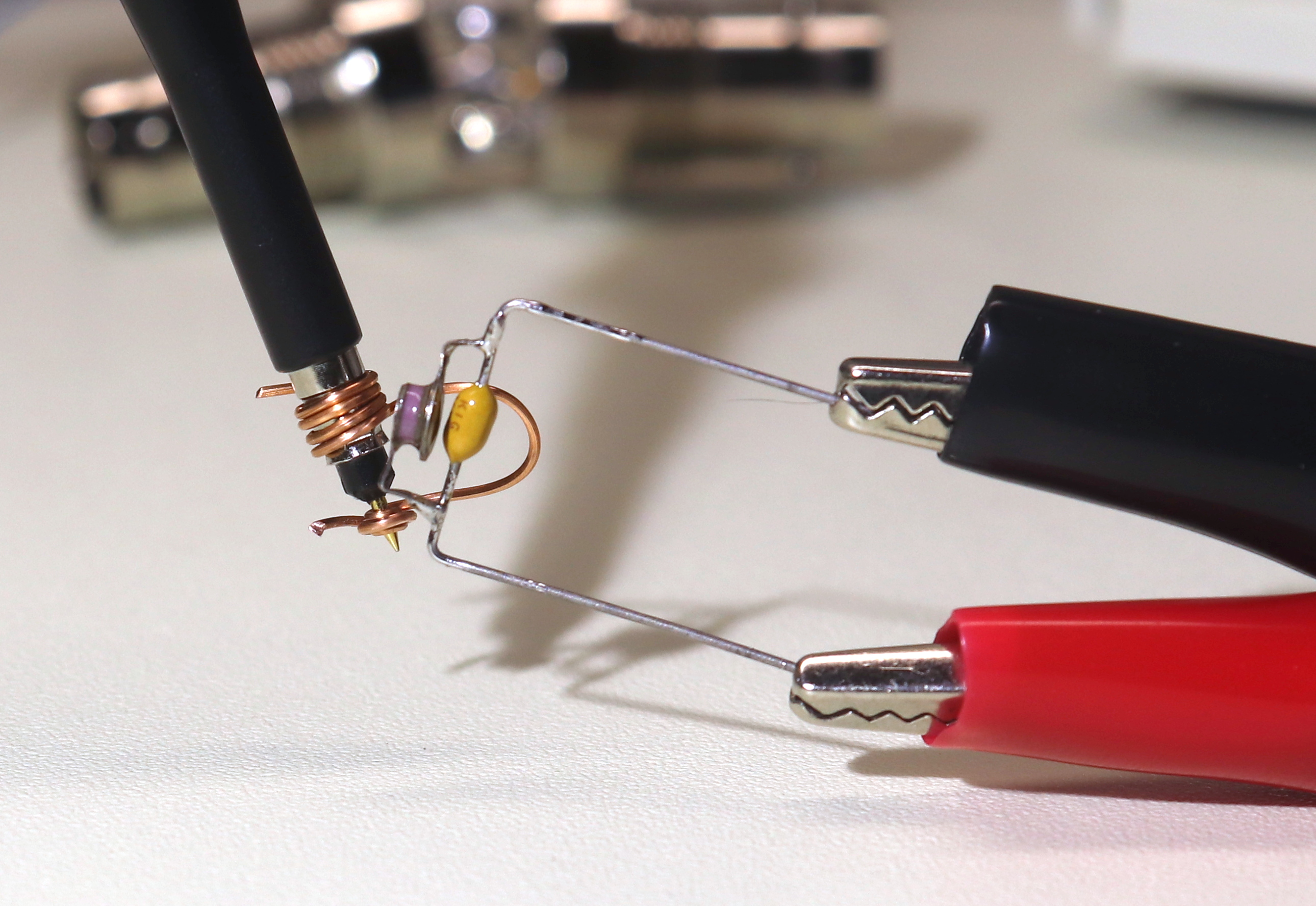
Not content with 300 MHz, I decided to strip the circuit down to the bare minimum to speed it up. I cut the diode leads short and soldered them directly to those of a 100 pF axial capacitor. In this case, the leads themselves are providing the necessary inductance, resonating with the diode capacitance. Again using a supply voltage of 700 mV, I found the circuit oscillated at 581 MHz. I’m not sure how to make this go any faster using lumped components – maybe someone can suggest a different method in the comments. Cavity resonators?
In any case, I find it amazing that a two-terminal device can form such an oscillator this simply. I also have a much greater appreciation for the designers who worked with these things: preventing unwanted parasitic oscillations in circuits using these diodes must have been a serious consideration. This is also why I haven’t tried to build an amplifier with these diodes (yet). There’s an old adage that the easiest way to build an oscillator is to design an amplifier, and now I’m wondering if this saying really caught on during the tunnel-diode days.
To measure this faster oscillator, I constructed a smaller pickup loop on the end of the oscilloscope probe with a length of bare copper wire. Don’t be fooled by the perfect-looking sine wave shape of the output; it’s a 581 MHz signal measured on a 1 GHz scope, so there’s not enough bandwidth to show many distortions. They may or may not be present, but we can’t tell with this equipment. And, like with the previous oscillator, the random coupling of the probe loop creates an arbitrary amplitude scale, so you can’t compare the outputs of the two circuits.
Hard Lessons
These gallium arsenide diodes are as fragile as they are fascinating. Of the four diodes I used in these experiments, I destroyed two. The first one was simply a matter of applying too much voltage during curve tracing. The best approach is probably to start low — the active region is below 1 V with these devices — and advance slowly. The second casualty was a case of overheating. The datasheet cautions to heat the leads no more than 3 seconds to a temperature not exceeding 260 °C, and to use a heat sink between the diode body and the solder point on the leads. I read this after having overcooked one. I didn’t have the recommended 2 mm wide copper tweezers, but finally made do with a clamp-on aluminum sink I originally bought for soldering germanium components.
The diodes are also static sensitive, and the datasheet ominously warns not to test them with a diode tester. I had already tested one with the diode-test function on a DMM when I read this, and although the diode seems to have survived — at least it was not instantly destroyed — the tester didn’t register the diode in either polarity. So, use the diagram in the datasheet to determine which end is which.
The bottom line: if you play with these diodes, be careful and make sure to buy a few spares.
Whats Next?
So, that wraps up this brief hands-on series about negative resistance devices. Be sure to let us know in the comments if you have first-hand experience with these unusual diodes or similar parts, especially if you can get one to go much faster than 581 MHz. I really want to see one of these things scream.


Four years ago I made two transatlantic (Ham) radio contacts (Morse code) with a homemade transceiver, entirely built from diodes as the only active devices. Two russian GaAs tunnel-diodes with 100mA peak current deliver the RF-power of about 5mW, while some american germanium diodes provide the AC-supply for the necessary audio gain on receive.
All details are on my QRZ.com page: https://www.qrz.com/db/dl3pb
The transceiver, meanwhile in a wooden enclosure, is now sitting on the shelf and waiting for better propagation on the 15m- band…
Peter
Yeah, but were they Russian contacts?
B^)
(Russian diodes, Russian contacts, nothing political here, move along)
If you’re going to play that game, I thought “American germanium” was kinda fun.
But back on topic: cool project…going to check that out now.
I missed that one!
Thanks for mentioning it.
p.s. I am jealous Yapo has a 1GHz o-scope!
I’ve got an old transistor and diode project book written by a ham from back in the late 60s-early 70’s. All the really cool projects (IMHO) use unobtanium tunnel diodes, unfortunately — even eBay has been very little help…
Those Russki diodes have too much lead inductance. I used ‘Murican diodes that had stripline leads (can’t remember the number, it was JEDEC registered though). They worked way up in the microwave region. They were surely going to replace transistors back in the day.
Read the GE T.D. manual: http://www.gonascent.com/papers/databook/tdmanual.pdf
I missed the first article where you introduced the makeshift curve tracer. It is possible to get the curve on the screen without post-processing, even if you can’t use the math channel.
It does, however, require that to oscilloscope and function generator do not share a common ground. You apply the signal to the DUT and sense resistor as before, but connect the scope ground to the junction between the DUT and the resistor. One channel measures the voltage across the DUT, the other across the resistor, where the last one measures negative voltage for positive current, so it just needs to be inverted.
There are other all-but-forgotten, esoteric parts out there, like the unijunction transistor, dual-gate MOSFET, diac, IGBT, and more…
IGBT’s are fairly modern and well-used aren’t they? Maybe you’re thinking of JFETs, triacs, and/or SCRs?
I wasn’t simply going for the old stuff. I actually left out JFETs, traics, and SCRs because they are so ubiquitous. I personally have never designed or used anything with an IGBT. I thought these were used for super high power devices, well beyond my reach. DIACs are typically used to gate TRIACs, but they have other uses. I just encountered the SiDAC in a Wikipedia DIAC article, which seems to be a higher-power extension of the DIAC, and may be used in applications similar to MOVs.
Another newish device is the 3-terminal memistor, similar to the 2-terminal memristor. Both depend on nonlinear operational characteristics (e.g. phase change). I have used neither, but some might argue that FRAM is a form of memistor (I have used TI FRAM uCs). Some might even argue that it was Stanford R. Ovshinsky’s early work on Ovionic memory that lead to so many of the newer memory technologies we see today.
And no telling what the future will bring once we lean more of the strange and quirky science of nanotechnology.
In my experience, computer power supplies “always” have IGBTs. Often sharing a heat sink with a pair of diodes.
I have not yet seen one there. In older devices BJTs are used and MOSFETs in newer ones. Perhaps super-high-power computer PSUs in the range of 1kW or more, use IGBTs.
Another one that never made the big time is the static induction transistor.
The original incarnation on the transistor is pretty funky too. Point junction transistors amplify on collector current not base current if I remember correctly. Weird stuff, you could build a stable memory cell with a single transistor.
Dual-gate MOSFETs are nowhere near unobtanium. You can easily get BF998 in almost every shop in any amount.
Back in the early 70’s I made FM “bugs” that fit into bottle caps using tunnel diode oscillators. They weren’t very stable and tended to drift in frequency quite a bit, but they were very small and simple to make.
These Zinc negative resistance devices are fun to play with: http://www.sparkbangbuzz.com/els/zincosc-el.htm
They are as described, black dots on a strip of galvanized steel sheet formed from oxidization with the flame of a propane torch (zinc fumes are bad to breathe in so do it somewhere outside with good ventilation).
They are easily reproducible (unlike the amount of time I spent trying to rectify am radio with a rusty razor blade), work best with two nine volt batteries in series with an additional series resistor to limit current to about 5 ma (more current will permanently destroy the negative resistance of the device). It is easy to solder the other end of the steel strip by sandpapering the zinc off of it just before soldering (steel will oxidize quickly to the point of unsolderability so sandpaper immediately before soldering). Then poke at the black oxide on the other end with a wire as described.
They ought to be good for at least a few megahertz.
Yes, for sure the easiest way to homemade (active) semiconductors. I built a transceiver for 3.5MHz with them, which delivers up to 1mW on a good day, but never made a contact due to the high noise level on the low bands and the lack of an efficient antenna for such low frequencies. At higher frequencies the signal becomes chirpy and power drops next to nothing. That’s why I recently built a passive, high efficiency (>90% at 1mW in) frequency doubler, which hopefully will allow a QSO on 40m band one day…
Don’t forget that the lowly Neon lamp (e.g., NE-2) exhibits negative resistance.
Furthermore, while you mentioned Nyle Steiner’s work with Iron Pyrite crystals, in the first installment, I have reproduced that work, only at audio frequencies, rather than at RF as Mr. Steiner has done (My webpage, where I reported this in 2005, is currently down, due to maintenance (incompetence?) by the ISP.).
There is also a considerable amount of literature, from the early days of radio, of “oscillating crystals”, such as:
http://earlyradiohistory.us/1920cry.htm
And, the Crystodyne:
http://earlyradiohistory.us/1924cry.htm
There are also mysterious references to “Amplifying Crystals” as far back as 1910, with some of the work done by Dr. W. H. Eccles (of Eccles-Jordan fame), and by Greanleaf Whittier Pickard.
http://earlyradiohistory.us/sec014.htm
Sadly, quite a bit of the work that Oleg V. Lossev (or, is it Losev?) did on solid state devices, including negative resistance devices, disappeared with him during the battle of Stalingrad, during WW2 (Some accounts have him disappearing in the burst from the direct hit of an artillery shell, while other reports have him simply starving to death.).
https://en.wikipedia.org/wiki/Oleg_Losev
Note that the amplifying crystals that Mr. Losev did his work with differs from what would become the Field Effect Transistor, invented by Julius Edgar Lilienfeld in the mid-1920s and early 1930s, well before the traditional transistor was invented two decades later (Sadly, the physics wasn’t understood until much later.).
https://en.wikipedia.org/wiki/Julius_Edgar_Lilienfeld
There’s some additional information on “Oscillating Crystals” from this British publication from 1925:
http://earlywireless.com/pdf/pw_xtal_experimenters_hdbk.pdf
For those who are devoted to this, they should probably pull a copy of H. K. Henisch’s book, “Rectifying Semi-conductor Contacts”, 1957, Claredon Press, Oxford, or the reprint/authorized-facsimile by University Microfilms, 1972, Ann Arbor, Michigan, which contains some of the physics behind the effects.
Oh, and finally, note that some Zener/Avalanche diodes will exhibit negative resistance, at some narrow portion of their operating curve (One researcher has indicated that between 75 and 80 percent of off-the-shelf Zener/Avalanche diodes exhibit the negative resistance effect!). Take a look at figure 5, on page 19, of On Semi’s “Zener Theory and Design Considerations Handbook”, and realize that those zigzags in the expanded portion of the curve represent regions of negative resistance. They call the effect the “microplasma discharge” theory.
https://www.onsemi.com/pub/Collateral/HBD854-D.PDF
Also, remember that there are even other negative resistance devices, such as IMPATT diodes.
Oh, yeah, some of the patents of some interest may be US755,840, US830,924, US929,582, US1,751,361, US1,751,362.
Dave
Unlike any solid-state device of which I am aware, the venerable NE-2 exhibits not only negative resistance, but it also emits light!
When I was a teen-ager, I got a bunch of NE-2s and resistors and capacitors, and a 67.5 volt battery, and made a relaxation oscillator “random twinkly light box” for my little sister for Christmas. It was great fun, and the current was low, so the battery lasted forever.
The 3I306M Russia Military Gallium Arsenide Tunnel Diode is really appaeling to some electronics application.
один – Pronunciation: [ah-DEEN] – Meaning: one
Find the replacement for Russian ‘и’ being ‘i’ in English strange. It’s always been a long ‘e’ sound to me. Wonder if there might be another reason for the substitution. I know it’s not important, but when I read the statement I had to go check if my memory of the Russian language was really that bad.
SCR’s are common in spot welders. They are water cooled and handle 800 to 1200 Amperes. Automobile plants use thousands of the SCR’s. They replace ignitron tubes previously used in spot welding.
Were you ever able to get the frequency to go past 581MHz? There are a few of the Russian diodes that have capacitances around 2pF so those should go much higher.