In the first part of this series, we took a look at a “toy” negative-differential-resistance circuit made from two ordinary transistors. Although this circuit allows experimentation with negative-resistance devices without the need to source rare parts, its performance is severely limited. This is not the case for actual tunnel diodes, which exploit quantum tunneling effects to create a negative differential resistance characteristic. While these two-terminal devices once ruled the fastest electronic designs, their use has fallen off dramatically with the rise of other technologies. As a result, the average electronics hacker probably has never encountered one. That ends today.
Due to the efficiencies of the modern on-line marketplace, these rare beasts of the diode world are not completely unobtainable. Although new-production diodes are difficult for individuals to get their hands on, a wide range of surplus tunnel diodes can still be found on eBay for as little as $1 each in lots of ten. While you’d be better off with any number of modern technologies for new designs, exploring the properties of these odd devices can be an interesting learning experience.
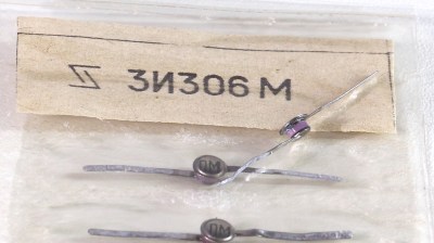
For this installment, I dug deep into my collection of semiconductor exotica for some Russian 3И306M gallium arsenide tunnel diodes that I purchased a few years ago. Let’s have a look at what you can do with just a diode — if it’s the right kind, that is.
[Note: the images are all small in the article; click them to get a full-sized version]
If you’ve spent any time on hackaday.io, you may have noticed that more than a few denizens of the site are fans of “alternative” electronic logic. Aiming to create digital circuits from such things as relays, vacuum tubes, discrete transistors, and occasionally diodes, they come up with designs that use these components in either antiquated or occasionally new and unexpected ways. This is exactly what [Mark Sherman] has done with his latest project, a single-transistor latch.
If you think every design has to compete with cutting-edge integrated circuits, or even must have an immediate practical application, you might as well stop reading now — and to play on the famous Louis Armstrong quip about jazz, if you have to ask why someone would do such a thing, you’ll never know.
Given that you’ve come this far, you’ll appreciate what [Mark] has come up with. It’s semi-well-known that the collector-emitter junction of a bipolar junction transistor (BJT) can exhibit a negative resistance characteristic when reverse-biased into avalanche breakdown. It’s this principle that allows a single BJT to be used as an ultra-simple LED flasher. [Mark] took this concept and ran with it, creating a single-transistor latch that can store one bit of information. As a bonus — or is it a requirement? — the transistor also drives an LED, so that you can visualize the state. We’ve seen a one-transistor flip-flop before, but that one also required diodes and an AC bias supply. In this new device, none of this is necessary, so it’s a step up according to the unwritten, unspoken, and generally agreed upon rules of the game.
In true hacker fashion, [Mark] came up with a working device without fully understanding exactly how it works. We, too, are a little mystified at first glance. So, [Mark] is asking for your help in replicating and/or analyzing the circuit. He explains what he has found so far in the video after the break, but the main questions seem to revolve around why the base resistor is required, and why it works with 2N4401s but not 2N2222s.
So, Hackaday, what’s going on here? Sound off in the comments below.
The concept of negative resistance has always fascinated me. Of course, a true negative resistance is not possible, and what is meant is a negative differential resistance (NDR). But of course knowing the correct term doesn’t do anything to demystify the topic. Negative resistance sounds like an unusual effect, but it turns out to be relatively common, showing up in places like neon lamps and a number of semiconductor structures. Now’s as good a time as any to dig in and learn more about this common principle.
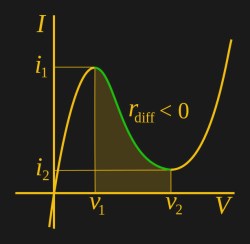
NDR means a portion of a device’s I/V curve where the current falls with increasing applied voltage. The best-known semiconductor device exhibiting negative resistance is the tunnel diode, also known as the Esaki diode after one of the Nobel-Prize-winning discoverers of the quantum tunneling effect responsible for its operation. These diodes can perform at tremendous speeds; the fastest oscilloscope designs relied on them for many years. As the transistor and other technologies improved, however, these diodes were sidelined for many applications, and new-production models aren’t widely available — a sad state for would-be NDR hackers. But, all hope is not lost.
Rummaging through some old notebooks, I rediscovered an NDR design I came up with in 2002 using two common NPN transistors and a handful of resistors; many readers will already have the components necessary to experiment with similar circuits. In this article, we’ll have a look at what you can do with junkbox-class parts, and in a future article we’ll explore the topic with some real tunnel diodes.
So, let’s see what you can do with a couple of jellybean transistors!
People talk about active and passive components like they are two distinct classes of electronic parts. When sourcing components on a BOM, you have the passives, which are the little things that are cheaper than a dime a dozen, and then the rest that make up the bulk of the cost. Diodes and transistors definitely fall into the cheap little things category, but aren’t necessarily passive components, so what IS the difference?
When you leaf through a basic electronics textbook, you’ll find chapters describing in detail the operation of the various components. Resistors, capacitors, inductors, and semiconductors. The latter chapter will talk about P and N type regions, introduce us to the diode, and then deal with the transistor: its basic operation, how to bias it, and the like.
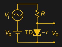
Particularly if your textbook is a little older, you may find a short section talking about the tunnel diode. There will be an odd-looking circuit that seems to make no sense at all, an amplifier formed from just a forward-biased diode and a couple of resistors. This logic-defying circuit you are told works due to the tunnel diode being of a class of devices having a negative resistance, though in the absence of readily available devices for experimentation it can be difficult to wrap your head around.
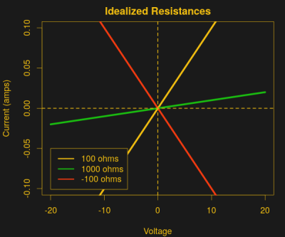
We’re all used to conventional resistors, devices that follow Ohm’s Law. When you apply a voltage to a resistor, a current flows through it, and when the voltage is increased, so does the current. Thus if you use a positive resistance device, say a normal resistor, in both the top and the bottom halves of a potential divider, varying the voltage fed into the top of the divider results in the resistor behaving as you’d expect, and the voltage across it increases.
In a negative resistance device the opposite is the case: increasing the voltage across it results in decreasing current flowing through it. When a large enough negative resistance device is used in the lower half of a resistive divider, it reduces the overall current flowing through the divider when the input voltage increases. With less current flowing across the top resistor, more voltage is present at the output. This makes the negative resistor divider into an amplifier.
The tunnel diodes we mentioned above are probably the best known devices that exhibit negative resistance, and there was a time in the early 1960s before transistors gained extra performance that they seemed to represent the future in electronics. But they aren’t the only devices with a negative resistance curve, indeed aside from other semiconductors such as Gunn diodes you can find negative resistance in some surprising places. Electrical arcs, for example, or fluorescent lighting tubes.
The negative resistance property of electric arcs in particular produced a fascinating device from the early twentieth century. The first radio transmitters used an electric arc to generate their RF, but were extremely inefficient and wideband, causing interference. A refinement treated the spark not as the source of the RF but as the negative resistance element alongside a tuned circuit in an oscillator, These devices could generate single frequencies at extremely high power, and thus became popular as high-powered transmitters alongside those using high-frequency alternators until the advent of higher powered tube-based transmitters around the First World War.
It’s unlikely that you will encounter a tunnel diode or other similar electronic component outside the realm of very specialist surplus parts suppliers. We’ve featured them only rarely, and then they are usually surplus devices from the 1960s. But understanding something of how they operate in a circuit should be part of the general knowledge of anyone with an interest in electronics, and is thus worth taking a moment to look at.
It is so often the case with a particular technological advance, that it will be invented almost simultaneously by more than one engineer or scientist. People seem to like a convenient tale of a single inventor, so one such person is remembered while the work of all the others who trod the same path is more obscure. Sometimes the name we are familiar with simply managed to reach a patent office first, maybe they were the inventor whose side won their war, or even they could have been a better self-publicist.
When there are close competitors for the crown of inventor then you might just have heard of them, after all they will often feature in the story that grows up around the invention. But what about someone whose work happened decades before the unrelated engineer who replicated it and who the world knows as the inventor? They are simply forgotten, waiting in an archive for someone to perhaps discover them and set the record straight.
Meet [Oleg Losev]. He created the first practical light-emitting diodes and the first semiconductor amplifiers in 1920s Russia, and published his results. Yet the world has never heard of him and knows the work of unrelated American scientists in the period after the Second World War as the inventors of those technologies. His misfortune was to born in the wrong time and place, and to be the victim of some of the early twentieth century’s more turbulent history.
[Oleg Losev] was born in 1903, the son of a retired Russian Imperial Army officer. After the Russian Revolution he was denied the chance of a university education, so worked as a technician first at the Nizhny Novgorod Radio laboratory, and later at the Central Radio Laboratory in Leningrad. There despite his relatively lowly position he was able to pursue his research interest in semiconductors, and to make his discoveries.