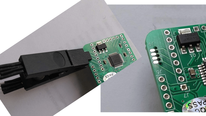
The problem is well-known: programming and debug headers consume valuable board space and the connectors cost money. Especially troublesome are the ubiquitous 100-mil pin headers, not because they’re expensive, but because they’re huge, especially along the z-axis. If you’re building miniature devices, these things can take up a ridiculous amount of space. With some clever thinking, [Simon Merrett] has found a way to re-use something many of us already have — an SOIC-8 test clip — to connect to a special footprint on the PCB without requiring another connector. He calls the system SOICbite.
The SOIC clip attaches to a footprint consisting of eight pads, four on each side of the PCB, plus five non-plated-through holes, which serve to anchor the clip in place. The idea of mating a PCB footprint directly with a removable connector isn’t entirely new — Tag Connect has been doing this for a while, but the connectors are expensive and single-sourced. On the other hand, SOIC test clips of varying quality are available from a number of vendors, including dirt-cheap deals on your favorite websites. The one disadvantage we can see is that the SOICbite footprint must be at the edge of the PCB to properly mate with the clip. The savings in space and cost may well make up for this, however.
[Simon] has made his KiCAD footprint available in a GitHub repo, and has offered to host footprints for any other CAD package there as well. So, fire up your preferred tool and draw one up for him to get these things widely adopted, because we think this is a great idea.
For the commercial alternative, check out our coverage of Tag Connect back in 2014.


Genius!
K.I.S.S. & elegant
Superb. Definitely going to use this!
I don’t like it. I prefer the Tag-Connect
I use and like the Tag-Connect as well. However, I see the beauty in this method. If you added a jig to the setup so that you can quickly slide PCBs in and out without having to think about alignment, then this would be even better. One thing I don’t like about the tag-connect is that after 50 – 100 boards my hands start to get tired from holding pressure.
This is good until you realize that that board probably goes into a box where you cannot fit the clamp unless you leave a large hole around that PCB area.
I have done something similar, but I used regular 2.54 mm spacing so that a simple dirt cheap header can be used to contact the pads. http://www.electrobob.com/autoresetrrr/comment-page-1/
I just use the standard thru holes and spacing then on the 2.54mm header I bend the pins slightly so that they go in the holes but they catch and friction holds them in. The same header is used on many boards and I have many headers.
It just works.
OK it’s no good for a production run of 10,000 but for a hobbist who can re-bend pins, it’s quick, and free and means no changes.
For the production stuff in the day job it’s pogo pins and custom board testers because 10,000 units.
Yes, bending works too, if a connector flat on the board is what you want. Also, pogo pins can be soldered on the pins and avoid bending of the header. They are quite cheap now.
instead of bending the pins I make the holes slightly offset from center in a zig zag so all the odd numbered pins are friction fit against one side of the hole and all the even numbered pins are against the other side
It’s a space thing (as is tag connect). This takes a lot less board real-estate than anything using .1″ pitch pins, be it as edge-connectors or through-hole.
I love the fact that I don’t need to buy a specific thing to make this work, the need to put it on an edge might be an issue occasionally, one solution would be to Make a small pcb and solder it on edge to the main board
Er… An SOIC test clip is easily and cheaply available to be sure, but it’s a pretty specific thing.
Great solution.
We use Redfit IDC SKEDD (e.g. 490107671012 available from digikey at $2) Works similar to the tag connect. Takes up more space than this SOIC solution though.
This part is rated “Minimum of 10 mating cycles”, but how many cycles it will reliably last in practice ? Because a programming/debug probe could reach hundred of cycles quickly in case of a small production.
It is kind of flimsy, but you can just make a bunch of cables and replace as necessary. It’s good for development/debug, not so ideal for production.
An engineer I worked with had two solutions to this issue. One was, of course, tag-connect. The other was to take a dirt cheap 8-pin board-edge connector (Think PCIe slot, but smaller), hacksaw out one edge, and design in a slot on the board beside the fingers. Tada, keyed low-profile 8-pin programming header.
We use the Tag Connect Header. It works great and has lasted for years. The only thing I do not like about it is during development, It can be difficult as a debug header. It wants to come out of the board.
I use the no-legs versions with the clip on the back side and it holds very well. That said, I’m adding a SOIC adaptor to my cart right now…
What I did is 3d print a bracket that looked like those sentries from Tron – legs go “around the board” and clip to the edge, and there’s a notch in it that holds the tag-connect cable to the board.
I like it, but…1.27mm IDC is great too.
Cool idea, it will work while board is not in the box. For the access from the top side it would probably be possible to use dummy SOIC package.
Now, if Microchip would get rid of that ridiculous RJ11/RJ45 connector on the ICDx programmers and replace it with a 0.100″ connector then we could have a decent way to use ribbon cable on the programmer end of the cable.
I’ve adopted this cheap clip for my projects: https://www.dfrobot.com/product-1307.html
It comes with 2.54mm pins and 2mm pins, so using the 2mm pins results in a pretty small footprint.
What footprint or part do you use to take advantage of the 2mm pins on your board? Eagle hopefully.
Does Eagle have 1mm dia test points? Just put them on a 2mm spacing for the layout and number of lines you need to connect. You can probably also use the 2×4 PTH pin header footprint with a 2mm spacing. Kicad certainly has these in the standard footprint library.
Very cool, I like it! For anyone interested in alternative or smaller programming headers, like the Tag Connect or other DIY options, I recently wrote a couple of articles about some alternatives here:
https://www.bigmessowires.com/2019/05/11/alternative-avr-programming-header-ideas/
https://www.bigmessowires.com/2019/05/13/more-avr-icsp-footprints/
I created a similar solution using a 6 pin spring connector from Digikey (WM11204CT-ND) and documented here: https://hackaday.io/project/25826/logs – have a look at logs Using the uProgrammer and Board Build and Bring-Up. This scheme has worked so well that I’m now designing a truly tiny arduino using it.
Idea: Use 4 Pogo pins and 2 Header Pins in a h-p-p-p-h-p configuration. Crappy visualization:
https://i.imgur.com/HAOvEpP.png
The Footprint (front) is in a straight 1.27 grid. The Pin Header on the left is shifted a bit, so friction may hold the rest down a little. The Pogos can be moved closer together if space is a constraint. And the footprint for the pogos don’t have to be vias but can be pads as well.
Bad idea?
This is the typical kind of thing you can patent
This. Is pretty brilliant! The SOIC clip ain’t that standard in the toolkit, but it is widely available.
It also solves the problem of Pogo-Pin/Tag-Connect systems in that they have to be pressed onto the target board constantly. This is just clipping on a Clothespin and done. Giving the same convenience as using a bulky 2.56mm pitched header.
Definitely Gonna port this design over to Eagle
Thank you – please could you submit a pull request on the SOICbite Github, once you have made it?
Sure thing! I cleaned my rough copy a bit to be proper Eagle library and have submitted a Pull Request. Also included Eagle render of footprint along with the device entry as it appears in the library
Merged! Thanks
No problem. Glad i could contribute to this neat idea! ^^
Sure thing! I cleaned my rough copy a bit to be proper Eagle library and have submitted a Pull Request. Also included Eagle render of footprint along with the device entry as it appears in the library.
thank you for sharing this article, I learned a lot from it
Thanks for sharing, it´s a great idea!
I thought it looked a good idea, BUT my SOIC clip does not fully close onto a 1.6mm PCB! That plus it needs an additional jig to align it. Hard pass from me, sorry! As mentioned above, a few pogo pins and pin headers to replicate the Tag Connect is a much better solution in my opinion.
I have been mulling over an ESP32 project where I wanted as smaller PCB as possible – this looks to be a good and affordable way of programming with a small connector footprint – brilliant.
Had a look through the schematics, GPIO2 is used in the SOICByte UART board footprint – but it doesn’t seem to be used on the programmer side. Does anyone know why it is included?
Doh, too many tabs open, wrong thread.