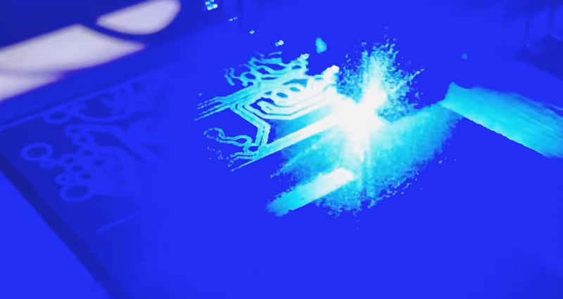
One of the more popular ways of rolling out your own custom PCB is to simply create the model in your CAD program of choice and send it off to a board manufacturer who will take care of the dirty work for you. This way there is no need to deal with things like chemicals, copper dust, or maintaining expensive tools. A middle ground between the board manufacturer and a home etching system though might be what [igorfonseca83] has been doing: using an inexpensive laser engraver to make PCBs for him.
A laser engraver is basically a low-power laser CNC machine that’s just slightly too weak to cut most things that would typically go in a laser cutter. It turns out that the 10W system is the perfect amount of energy to remove a mask from a standard PCB blank, though. This in effect takes the place of the printer in the old toner transfer method, and the copper still has to be dissolved in a chemical solution, but the results are a lot more robust than trying to modify a printer for this task.
If you aren’t familiar with the days of yore when homebrew PCBs involved a standard desktop printer, many people still use this method, although the results can be mixed based on printer reliability. If you want to skip the middleman, and the need for a chemical bath, a more powerful laser actually can cut the traces for you, too.


This works great with Hackerspace class CO2 machines.
Clean board very well(scouring pad), two light coats of spraypaint, laser off, wash and etch. We’ve been comfortably doing 0805 single sided boards. Nice to see it working with smaller machines too.
Just remember: Acrylic paint, so you don’t damage your machine. :)
Yep, we used spraypaint as well. Alignment was still fun.
I’ve done this before, the only problem I have is trying to get the drill holes to be lasered out. SVG plugins I’ve tried ignore them.
Eagle has a ulp to add the holes
It’s been a couple years, but I used something that converted eagle pcbs to svg, so have the added some new stuff since?
I’ve done this sort of thing with my smoothie-equipped 40W CO2 laser – enamel spray paint works fine instead of brushing on, and cleans away easily with solvent when done etching. However, speed just doesn’t compare to toner transfer (which I use actual transfer sheets for, not photo paper or glossy ad newsprint).
Oh, and what’s up with “This way there is no need to deal with things like chemicals” – er, the “chemicals” would be the etchant, which is the step after lasering the mask…
That sentence clearly is talking about sending the board off to a manufacturer.
I managed to make my own PCBs at home with a standard cheap HP Deskjet 3630 and get a fpc 40-pin connector with 0.5 mm pitch to fit on the board with some decent pads. However, 0.5 mm takes some real printer calibration and an expensive laser printer is an optimal choice for this task. I did the good ol’ UV and photo resist etching and wouldn’t call it “expensive equipment”.
Why burn the coat instead of using a lower power laser and expose photosensitive PCBs? Would be more reliable. This process here doesn’t seem to be very detailed and reliable.
I agree that using a photoresist would be a much better choice compared to ink.
One chemical less, one step less. Also no need to coat with photoresist or buy pre-coated, so it’s 2 chemicals less. Reasonable benefits.
Photoresist and sensitized PCBs are much more expensive than a coat of paint, the paint having the additional advantage of being available at the local hardware store. Anyway, I’ll be trying this method although I have had no issues when using the toner transfer method.
I wonder if it is better to drill the board before etching it.
If you use a CNC machine to drill, it would avoid ripping pads and tracks.
Just classifying, if you use photoresist film, you can drill holes before etching. Then you can apply the film in both sides. The film will cover the holes, preventing side etching.
This is basically the same steps used by pro pcb. Applying the solder mask is also a photographic process, but it requires a curing process (a electric oven does the trick).
The only thing missing for a pro level pcb would be plated holes, but that’s a whole new level. I consider it pointless to do this at home.
One last tip: stop using ferric chloride. A great alternative is this:
https://www.instructables.com/id/Stop-using-Ferric-Chloride-etchant!–A-better-etc/
Do a search for decal pro fx fab in a box kit.
Just finished a laser safety training course, pretty sure that the laser machine he is using would be illegal in the EU and probably the US too. If you are thinking about putting one of these in a workplace or hackerspace I recommend you look up your legal responsibilities and check that your machine complies with the relevant safety standard (IEC TR 60825 in the EU). I would also think long and hard about your fellow house guests too if you are thinking about putting one of these in your home, to my knowledge they don’t make laser safety goggles for dogs. One last point, you also need to be aware of the increased fire risk from stray reflections.
I think it’s a little irresponsible from Hackaday to be promoting these sort of articles without including a disclaimer about the dangers of converting 3d printers to laser engravers.
https://www.lasersafety.com/resources/laser-safety-by-industry/veterinary/
I stand corrected.
Did you see these ones there? haha
https://www.lasersafety.com/product/elm-f5p01-5001/
TC76 (the people that write the IEC825 series and other stuff) have never published a ‘general’ technical report for the series. The standards that are used for national harmonization and that can be used as a basis for a presumption of conformity would be based on IEC61010-1 and IEC60825-1, -4, -13, -16, -19; and the applicable Technical Reports (which are not normative and should not be a TRF reference) would be -4, -10, -14.
Per 29CFR1910, it would only be illegal for use by a hobbyist where not used in a work place subject to OSHA regulations.
For the EU, look at the 2014/59/EU directive to determine whether a home-built unit would be scoped. The Low Voltage Directive is the only marking directive that would apply to home-built stuff or consumer stuff.
I am an idiot.
“Per 29CFR1910, it would only be illegal for use by a hobbyist where not used in a work place subject to OSHA regulations.”
should be
Per 29CFR1910, it would be illegal for use by a hobbyist only where used in a work place that is subject to OSHA regulations.
Spinning a board at home seems less and less worth it. I’ve been through the process many times, but via’s and through hole plating are severe limitations. Although you can search HAD for through hole plating options, neither chemical plating nor rivets are great options. Being able to spin boards has saved my butt a few times when I need a prototype for a demo faster than JLC can get it to me, but without a way to connect both sides of the board, the time invested just isn’t worth it.
There are plenty of reasons to spin a board at home, though the more complex the board is, the more involved it becomes. Certainly not feasable for >2 layer boards, and less so for high speed stuff.
Some reasons to do it instead of (or at least BEFORE) sending off to a fab:
same-day turnaround
you need just one of something for a test
better than perfboard or breadboard (esp if you’re using SMD parts)
cheap
Sure, you might be thinking “but you can order 10x 100x100mm PCBs from jlcpcb. elecrow, and others for a couple bucks plus shipping.” True, but even if you pay (extra) for expedited shipping, you’re looking at getting them within a week (IF it doesn’t get held up at customs). How does that compare with 30m from now? If you find something wrong with your design NOW you can bodge the test board, correct the design, make another, and *THEN* send it off to a board house.
Laying out a board – possibly with a different layout than your final might be (I personally find that single-sided PCBs are less fiddly for alignment, and 0R resistors are great for assisting with 1-sided routing) is straight forward, and can get you a functioning circuit to physically experiment with before making a final PCB and sending it off for fab. Even if it’s not your entire design – just part of it.
If you’re providing the PCB to someone else, and want a polished result, by all means, pony up for express shipping and some spiffy solder mask for your first go. If you’re like the bulk of hobbyists that want to make something, or experiment, home etching is totally worth the effort – at least for designs that fit within the design limitations of the process.
I tend to agree. I can’t remember the last time I could or would be satisfied with a layout needed to make something work on a single side. I have a bit of a fixation with small pitch packages and cramming everything in the smallest board possible, so things like rivets aren’t an option. I did the thin wire strand between sides before, and the frustration was always more than the wait to get a PCB made up proper.
I can see situations where it’s viable/preferable though, I just don’t have that need.
I’m doing the same with PCB wizard and a laser 2W, now I’m in the process of solder mask that works well. The engraving process last 7 minutes for a PCB 5.0X5.0 cm + 10 minutes Etching time. The Sharpie process can’t be used to get 0.7mm traces.
I bet that after chemical etching, you can add new coat of acrylic spray paint as solder mask. Then use laser again to reveal the pads, while leaving traces under the paint.
Guy here doing just this:
https://www.youtube.com/watch?v=kpk1qH6_aD4
Wrong link ?
Nevermind. It showed up after I posted the comment.
This is just another reason for me to want to get a laser cutter/engraver even more …. like I don’t have enough projects and a shed full of tools :lol:
An interesting experiment here with Galvos –
https://youtu.be/EUXemgF8qV0
I’m interested to know more. What laser do you use? What type of paint do you apply to the PCB? What line/spacing do you achieve?