In a recent article in Nature, you can find the details of a RISC-V CPU built using carbon nanotubes. Of course, Nature is a pricey proposition, but you can probably find the paper by its DOI number if you bother to look for it. The researchers point out that silicon transistors are rapidly reaching a point of diminishing returns. However, Carbon Nanotube Field Effect Transistors (CNFETs) overcome many of these disadvantages.
The disadvantage is that the fabrication of CNFETs has been somewhat elusive. The tubes tend to clump and yields are low. The paper describes a method that allowed the fabrication of a CPU with over 14,000 transistors. A wafer gets nanotubes grown all over it and then some of them are removed. In addition, some design rules mitigate other problems.
In particular, a small percentage of the CNFETs will become metallic and have little to no bandgap. However, the DREAM design rules can increase the tolerance of the design to metallic CNFETs with no process changes.
Before you get too excited, limitations in channel length and contact size keep the processor running at a blazing 10 kHz. To paraphrase Weird Al, your operating system boots in a day and a half. The density isn’t great either since working around stray and metallic CNFETs means each transistor has multiple nanotubes in use.
On the other hand, it works. New technology doesn’t always match old technology at first, but you have to crawl before you walk, and walk before you run.
We imagine you won’t be able to buy this for $8 any time soon even if you wanted to. At 10 kHz, it probably isn’t going to make much of a desktop PC anyway.


“However, the DREAM design rules can increase the tolerance of the design to metallic CNFETs with no process changes.”
It is a bit silly for both Nature (and other outlets) and the ones making the paper to call it “DREAM” as if it were something special… It isn’t. All it is, is the simply fact that transistors and circuits have noise, and metallic CNT adds onto that noise, making it worse, and the design rule is therefor, “Do not have large complicated logic structures.”
As an example, we can build an N input OR gate, but as we increase the number of inputs, eventually the gate becomes so large that the noise itself is able to change the outputs. This is an undesirable effect. Solution is to built the big OR gate using a composition of smaller OR gates instead. Downside with this is that now we have more transistors in series for the signal to pass through, and thereby a lower max system clock speed can be realized.
This is true for all technologies, be it CMOS, TTL, vacuum tubes and even relays. (but one needs a lot of noise to transition a relay) So the “DREAM design rule” is absolutely nothing new to speak of. And it is heavily used in all fields of electronics, be it RF engineering or blinking a bunch of LEDs. (So the paper shouldn’t really be given credit for it.)
Also, the statement: “A wafer gets nanotubes grown all over it and then some of them are removed.” is not what is described in the paper.
The paper describes a process where a CNT suspension (yes, CNTs suspended in a liquid, fancy stuff that is) is poured over the wafer (the wafer has a photoresist layer on it, so we only get the CNTs were we desire), then the wafer gets gently rinsed, since CNTs adhere better to the wafer when alone then when bundled together, thereby the bundles can literally be gently washed off, before the coating step gets another go, and so forth until the wafer has no bundles to speak of left. Then one chucks it over the cubicle wall to the next production step per say.
Also, the speed a processor runs at is rarely only held back by the transitioning speed of transistors used to build it. But also by how many transistors in series needs to transition for a given clock cycle to finish. And as mentioned above, if more advanced logic implementations needs to be broken down into smaller simpler pieces to get enough stability for it to work, then this will also decrease the peak processing speed. Then there is signal routing and integrity, parasitic in the interconnects, then there is power delivery/stability.
In the end, the fact that the chip is more a “proof of concept” then anything else, means that it could work at 1 Hz and be just fine… Since the thing it tries to prove isn’t the performance of CNT transistors (that has already been proven by others), but rather that one can build tens of thousands of them at once. And potentially millions of them too. But that is for the future to prove.
Another thing the paper also puts forth is the fact that they do a fair bit of cold process steps in their manufacturing, and that the CNTs themselves provide the semiconducting portion of the circuit, meaning that the substrate could be practically anything that is reasonably flat. Doesn’t need to be an expensive monocrystalline silicone wafer. Also, since there is no need for a semiconducting substrate to built it on, we can also construct a second layer of CNT transistors on top of the first. And a third on top of that and so forth. This combined with potential power efficiency improvements of CNTs, would enable more complicated 3D semiconductor technology to be built in the future.
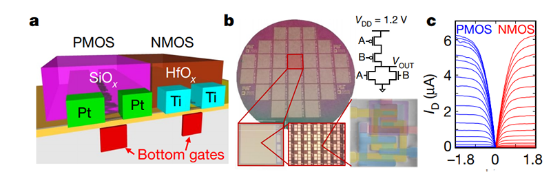
Though, I do find it interesting how they dope the CNTs to form P channel and N channel devices. Since one can’t easily substitute atoms in a carbon nano tube. So the researchers turned to atomic layer positioning of oxides, these would either donate additional electrons to the CNT or steal electrons from it, depending on the composition and type of oxide used.
In the end, the paper is an interesting read.
Even though there are other technologies on the verge with potentials of their own.
I don’t see the point, the goal is reduced thermal profile, greater thoroughoutput, lower cost of manufacturing.
Yes, I know what is going on. That’s their problem not mine.
RISC is good ;-)