One of the step changes in electronic construction at our level over the last ten or fifteen years has been the availability of cheap high-quality printed circuit boards. What used to cost hundreds of dollars is now essentially an impulse buy, allowing the most intricate of devices to be easily worked with. Many of us have put away our etching baths for good, often with a sigh of relief.
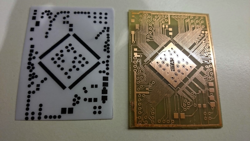
We’re pleased that [Riyas] hasn’t though, because they’ve etched an STM32 dev board that if we didn’t know otherwise we’d swear had been produced professionally. It sports a 176-pin variant of an STM32F4 on a single-sided board, seemingly without the annoying extra copper or lack-of-copper that we remember from home etching. We applaud the etching skill that went into it, and we’ll ignore the one or two boards that didn’t go entirely to plan. A coat of green solder mask and some tinning, and it looks for all the world as though it might have emerged from a commercial plant. All the board files are available to download along with firmware samples should you wish to try making one yourself, though we won’t blame you for ordering it from a board house instead.
It’s always nice to see that single board computers are not the sole preserve of manufacturers. If the RC2014 Micro doesn’t isn’t quite your style, there’s always the Blueberry Pi which features a considerably higher penguin quotient.


I clicked through to the actual article, and if that came from a professional fab house, heads would roll. It’s still better than what I could make at home, admittedly.
Well, the etching looks pretty good to me, but I can only guess that things went severely south sometime during the solder mask stage. In theory, you can do all of the steps involved in a multilayer board with CNC routed edges, through-hole plating, and solder mask and silkscreen on both sides, but every step is something else to screw up, and THIS is what makes cheap PCB fab services a real win.
Okay, it is indeed a nice etched board. And having etched more then a few boards myself over the past decades I’m aware of the possible problems. The statement: “that if we didn’t know otherwise we’d swear had been produced professionally” did make me giggle a bit at first. But then I started to think and considering the pitch involved this is indeed a very nice etching job and doing this at home isn’t that easy. So a job well done. Regarding the green soldermask, I wonder if it’s really worth the trouble. Sure, it results in a green PCB but it doesn’t make it look that much better and I wonder if it really helps for soldering. Personally I would cover the whole PCB in a thing layer of tin, some flux, a large iron and solderwick that has soaked up some tin. That works surprisingly well and may even fix small etching problems, although the PCB mentioned here doesn’t really need that. An etching job well done!
Having soldered both bare boards and masked ones I can say that solder mask makes life MUCH easier. It helps when using solder paste (for SMD stuff) as any excess paste simply beads up on the solder mask after heating and can be scrubbed away without risk of shorting any pins. It also means bare copper is seen only where things get soldered to, so it acts as a bit of a reminder to help you avoid putting in say, a grid of resistors at 90 degrees to where they should g (connecting between the wrong pairs of pads. Having soldermask also lets you have silkscreen writing on the board, really helps with labelling as a reminder of what component goes where, provides a double check alongside a large (say A3) printed diagram when positioning components.
Silkscreen does not require soldermask. I’ve seen quite a few PCBs made before the wave solder days, that had not one, but TWO colors of silkscreen on them. Of course, silkscreen is a lot of bother if you’re only making one or two copies of a board. Unless you’re NASA, in which case EVERYTHING is a lot of bother.
oh, don’t get me wrong here.
A soldermask is a great plus on any PCB but only IF applied the properly. As you can see in the images on the projects website, it’s all over the place. It’s even on the pads itself, the place where solder is to be applied… so it first needs to be peeled/scraped/sanded off in order to be able to solder. If the soldermask would or could be burned off (and there are versions that allow you to do that (or at least there were 30 years ago) then it would most certainly NOT result in a pleasant solder experience. And in those situations, it would be better NOT to apply a soldermask.
BUT, if you do are able to apply a soldermask properly, please do!
The solder mask also helps to anchor traces/pads to the FR4 especially when the traces are thin and pads are tiny. Even a cheaply board with solder mask can survive a couple of rework without the pads peeled off. Can’t say the same for home etched bare board.
Yeah, you absolutely need to take the pitch into account on this one. When you zoom in and realize just how small those traces really are, you get a new appreciation for doing this DIY.
This may be the best homemade circuit board I’ve ever seen. Was the board resist supplied on the board or sprayed on? What was the etching solution? What was used for the negative, was it plotted on film as a direct transparency or photo?
I’ve done a bunch of kitchen table prototype circuit boards and I’m not sure if I would even try this. Good job.
a good tip when printing on film is to make 3-4 copies. stack, align and fixate the films. make sure toner is closest to the pcb. this method makes the uv exposure part prone to less fails and not so sensitive to over exposure. also small print errors with missing toner is neglected.
6/6 is certainly possible with UV, and even Press’n’peel. But what lets all DIY etched boards down is lack of plated through-holes (rivets work, but are expensive and a pain for doing 100+). And considering a board this size can be had for $5 (for 5 quantity) I’m surprised people still make their own boards for anything other than unusually large ones.
Turn around time? I am probably crap, but it takes me 3 or 4 iterations to get a board right. Easier done at home where possible, I discover the errors the same day!
I do also worry about how the chinese vendors achieve such a low price. Are the noxious substances really being properly handled? Here in the UK, correct disposal is a headache – and very limited in volume, residentially. Which is why I do cnc boards if I can.
I make sure things are designed up front and not left to “debugging”. Most of my hardware projects tends to work the first time and if not only require a 2nd rev or mod.
A extra week of looking over the design or layout *before* sending it off pays off easily. Randomly throw money at things and hope they work is a waste of my time and money. It gets far worse for work projects as you’ll be wasting customers’ time and money.
Hard to simulate everything unless you arr dealing only with parts you know very well
I believe too in multiple PCB revisions unless you are okay with some rework
Hardware unlike software has a cost and time factor. There are ways of doing more rigorous engineering to minimize churns. I try to do as much up front work as I can so I don’t end wasting my time figuring after the fact.
Unless there are problems or refinements that require design changes, you should have figured out all of the silly mistakes after rev 1 from testing board before moving on the next rev.
Most of the hobby level design I looked at (HaD.io, OSH Park PCB) are not high complexity. Few have ventured far from well known parts either. Most unfortunately don’t try to design thing properly and do their homework before pushing out to schematic. Few even bother reading official sources uch as datasheets/app notes/reference designs as they would rather trust unreliable 3rd parties by watching some youtuber or go on social site to ask for advice. Chinese whispers in engineering doesn’t work.
I don’t see the point. For much less time wasted and trouble one can order even more complex boards from China. With better quality. I abandoned etching at home because it was too unreliable a process and wasted too much material. I can easily order either CNC boards from local suppliers, do it myself with my CNC after a simple mod, or just buy them from China, with metalization, tin coat, silkscreen, etc. for less than I spend on food per day…
I also did design a “expose all pins to headers” board for PIC24/dsPIC/PIC32 chips. I can’t finish the project though because my eyesight is too poor to solder TQFP64 without visual aid, which is expensive here…
If you have access to a cnc, surely you can improvise a visual aid? If you can’t make or buy a lens, USB microscopes are very inexpensive (at source, import taxes not withstanding)
I have a specific lens and donor webcam to make such a microscope, but I don’t have a specific tap to cut a matching thread. The tap is just extremely rare in my country. Also I have a life, and plenty of it, so I need to prioritize project by their profit margin. For now I’m making puzzles under a brand of PineKio, which you can find on Ebay.com…
Your products don’t show up on ebay UK fyi. A shame, given that you’re also in Europe.
It should: https://www.ebay.co.uk/sch/i.html?_nkw=pinekio&_blrs=spell_check
I don’t know if it is the same as what the original point is, but I grow some of the best tomatoes at home and they only cost me about $4.00 each. I have a friend who makes furniture and another one who does stained glass. The tomatoes are available from Mexico very cheap, the furniture is available for an excellent price from North Carolina and as much stained glass as a person could ever want comes for pennies from China.
I think the point is one of these Walt Whitman kind of things.
The craftsmanship speaks for itself.
Besides, I’ve always wondered when you send out digital circuit board files for a commercial product prototype to China what happens to these proprietary designs in the future.
They’ll have a hard time figuring what you are doing for anything mildly complex involving a few programmable devices. It is not like you give them a schematic, BOM, and bitstreams for the devices.
In case of PCB making all the craftsmanship is in design, not in manufacturing. And no matter how much time you spend on developing your etching skills or improving the technique, you won’t achieve the same quality to costs and time ratio as even the basic PCB making firm from China…
I have a book about electronics from ;ate 1970s. The proper method of making PCBs according to it is to use strips and circles of adhesive foil to create the circuit by hand, fix some details and make curvy traces by using a dispenser of special lacquer (pine resin dissolved in 90% alcohol) made from syringe and needle, and then etch it in FeCl solution or in acid. True masters of this technique were able to make complex two-sided boards by hand…
Gerber files sent to Chinese board makers don’t contain the values or part numbers. Unless you are ordering full assembly and programming of your product, or you made an open source project, they won’t copy it. They also won’t copy anything that doesn’t sell at decent rate…
You mean something like this? https://www.aliexpress.com/item/32332672453.html
These boards come with soldermask, so reflow is easy and doesn’t require a perfect alignment. I would never dare trying to hand-solder something like this.
I do understand your frustration with your eyesight very well. Until 10 years ago I could not understand why anybody would ever want to solder under a magnifier or a microscope. No problems reading the markings on 0603. Now I am happy if I can even find a 0603 again that slipped of the tray… :-(
My design was made for TQFP-64 parts only. Microchip has few families of PIC24/dsPIC/PIC32 chips that share pinouts, so on the board there is voltage regulator, filters, LC filter for analog part of chips, decoupling capacitors, etc…
The smallest part I soldered by hand was a 0402 resistor, which I did by feel, not by sight…
Since the advent of SMD, to continue in this hobby has mandated one learn CAD and PCB mfg as well as going on a quest for some manner of microscope. Essentially you need to learn a couple different hobbies in order to practice your target interest of learning/doing electronics and building what you’ve imagined. Early days it was a shoestring budget. Now it’s “an investment”. The investment needed will continue to grow until out of proportion, which for many it already is.
Since the 50’s most projects have been designed, built, then receive several iterations of change and adjustment. Those required changes will now oft be ordering a new board as we already experience.
The lucky part is, anyone enthused enough by electronics to take it on as a hobby will also have several other hobbies at the same time, so losing one hobby is not a total disaster.