If we had a dollar for every exciting new device that’s promised to change everything but we never hear of beyond the initial hoopla, we’d own our own private islands in the sun from the beaches of which we’d pick out Hackaday stories with diamond-encrusted keyboards. The electronic engineering press likes to talk about new developments, and research scientists like a bit of publicity to help them win their next grant.
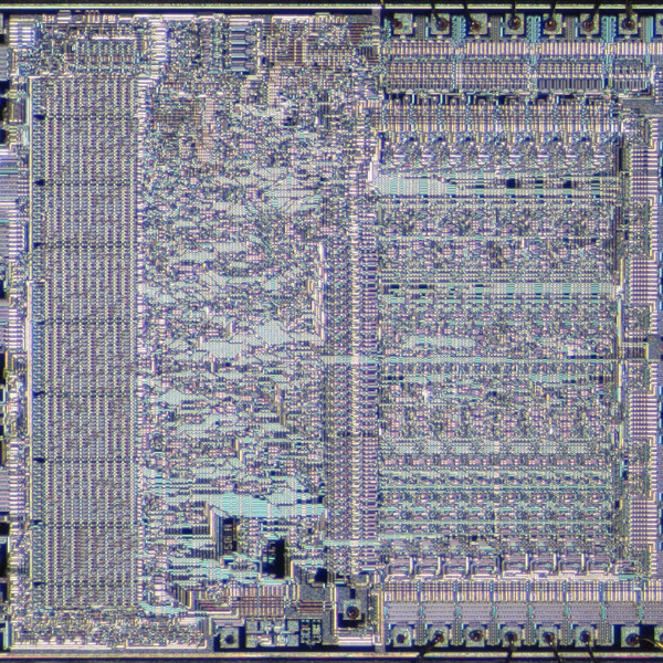
The Bizen transistor however sounds as though it might have some promise. It’s a novel device which resembles a bipolar transistor in which the junctions exhibit Zener diode-like properties, and in which the mechanism is through quantum tunneling rather than more conventional means. If this wasn’t enough, its construction is significantly simpler than conventional semiconductors, requiring many fewer support components to make a logic gate than traditional CMOS or TTL, and requires only eight mask steps to manufacture. This means that lead times are slashed, and that the cost of producing devices is much reduced.
The device’s originator has partnered with a semiconductor fab house to offer a service in which custom logic chips can be produced using the new devices in a series of standard building blocks. This is likely to be only of academic interest to the hacker at the moment, however the prospect of this cost reducing as the technology matures does show promise of reaching the means of some more well-funded hacker projects. It will be a while before we can order a chip with the same ease as a PCB, but this makes that prospect seem just a little bit closer.
Thanks [Ken Boak] for the tip.


“logic hate” ?
seriously you couldn’t reason it was supposed to be “gate”?
“Assumption is the mother of all fuckups”
:o)
+1
That’s a pretty big assumption.
that’s one way to justify your own inadequacy.
Without assumptions science would never make any progress.
Why doesn’t this website EVER make corrections?????
Misspelling iz hakking teh langwage. Down wiv c0nf0rmity!
This made my night
Yeah right? They never make corrections, ever…geez!
(fixed)
10 q
:o)
+won, Mike! ;-)
Sometimes they do. I’ve seen where someone commented on a spelling error that did no longer was in the summary and the author responded with “fixed it” or something like that.
Once someone has commented though, the fact it happened is pretty much permanent knowledge so why bother? Fix it AND delete the comment and the comment section errupts. Oh the censorship!
It’s the English spelling. It doesn’t make any sense. And thus spelling mistakes don’t make sense either. So there is nothing to correct. :)
I’m pretty sure they don’t mean “hate”. But I’m convinced that hackaday uses the latest tech in spelling checking and relies on it to trigger on silly errors, and this is technically not an error. Though I’m sure they meant something else. A nice example of the wonders of spelling checker technology and that it cannot be trusted… is demonstrated in the infamous poem below:
Eye halve a spelling chequer,
It came with my pea sea,
It plainly marks for my revue
Miss Steaks I kin knot sea.
Eye strike a quay and type a word,
And weight four it two say,
Weather aye am wrong oar write,
It shows me strait a weigh.
As soon as a mist ache is maid,
It nose bee for two long,
And I can put the error rite.
Its rarely ever wrong.
Aye have run this poem threw it
Iamb shore yore pleased too no,
Its letter perfect in it’s weigh.
My chequer tolled me sew.
🤣 👍👍👍
> requiring many fewer support components to make a logic hate
Not sure what logic hates, but I can sympathise ;)
Maybe the toaster in Red Dwarf was made from those gates.
Certainly the Dalek are full of that stuff
My first wife. The feeling was mutual. :grin:
“a logic hate” ?
hate is not logical :-P
The real question is what does logic hate? Analog?
No, DIGITAL hates analog while analog has a trans-electric love for logic.
The linked sites are in the same “vain” ;-)
“Microporcesor architecture”
“SFN has developed its own unquie …”
at the EETimes site, the caption : “maser slave”
oh my… the save on layers AND letters :-D
That is sort of like an emitter follower circuit, but with masers.
And don’t forget the “maser slave” flip flops.
I know… I should have refreshed this page before posting…
and more people should proofread ;-)
Always interesting to hear about new transistor implementations and improvements in the field.
Though, 8 mask layers is rather complicated. considering that a bog standard BJT can be built with only 3 mask layers, 4 if you want both NPN and PNP on the same chip, or FETs, 5 if you want both types there as well. Now, one can need additional mask layers if one desires more exotic dopings and both high and low voltage rated transistors, etc…
Sure it weren’t 8 mask steps for the whole chip?
You are forgetting about some details like interconnects, vias, passiviation…
A discrete bipolar transistor needs at least 4 layers. The old NMOS logic processes got away with 6-8 for single poly/single metal, depending on wether depletion devices and buried contact were needed.
8 masks is still low for a modern logic process. It looks like it is dual metal, even.
The problem is that at some point mask costs become irrelevant because you still have a significant cost overhead for software, assembly, qualiication, testing…
I am though of the opinion that interconnects, vias and passivation layers aren’t parts of the transistor itself, and therefor shouldn’t be included in the layer count of the transistor.
Since a chip can have as many interconnect and via layers as the manufacturer desires. (though at increasing costs and lowering yields, but one can still go to tens of layers if one is “crazy”…)
After all, I wouldn’t have ended my original comment with “Sure it weren’t 8 mask steps for the whole chip?”
Though, re-reading the article they aren’t actually talking about the individual transistor, nor the whole chip. But rather just how many layers one needs for a typical logic gate.
Searching around a bit on the topic myself, the suggested transistor implementation can build a 3 input NOR gate with only 4 mask layers, and that is fairly impressive, though, the 66% size reduction compared to CMOS is also interesting.
8 layers were only stated in the eeTimes article as “Increasing to eight layers brings high power, high current switching capability.” And there one got to question what they mean, is that 10mA, or 1A? (“continuous”) Main application would likely be IO drivers. Communication on the chip itself rarely needs much current at all. (And one wouldn’t really use digital logic for high power switching applications…)
In the end, all of this is though totally pointless information for the vast majority of chip makers. Since the main two questions hasn’t been answered.
What is its power consumption over frequency? (Smaller transistors doesn’t make modern chips smaller, since the the transistors are intentionally spaced out from each other to make the chip easier to keep cool.)
And what is its transition-frequency/switching-speed? (Not that it is hard to reach 10+GHz to be fair.)
But taking into consideration how the Bizen transistor promises to be able to include multiple gates in one transistor. (all sharing a common output) Then this should mean that we have fewer switching devices to start with for a given design.
So if it keeps the same power consumption as current CMOS technology, then we would see lower power consumption there already. And a more tightly implemented chip as well.
And since we have fewer transistors for a given piece of logic, then we most likely have fewer transistors in series for our signal to progress through, effectively meaning that if the transistor keeps the same transition frequency, then we can expect a higher end frequency for our logic. (unless propagation delay in the interconnects already make up the majority of the clock cycle.)
So it could be an interesting future technology, or just another “cool” thing that quickly gets forgotten. Depending on how it performs. After all, it might stop working at sub 30nm. (Test chips have so far only been made at 1µm, so who knows.)
So, it is electrically equivalent to a JFET, but it functions a little differently, correct?
Josephson junctions are coming :-)
It’s so cool, it’s a Bose-Einstein Condensate ;-)
Graveyard for photons.
So if I boil Bose-Einstein Condensate, I get Moonshine?
Besides all the “what does logic hate” comments, this one is one of my favorites!
ehm.. so what can you do better with transistor compared to for instance BJT or MOSFET?
You can advertise your “cutting edge” technology in brochures…
Some are listed here: https://www.wafertrain.com/index.php/theprocess/the-process
But the others I’ve seen mentioned are:
~5x reduction in manufacturing time
~3x higher gate density
higher switching speed
lower dynamic power
allows AC signals – which could be useful for Gallium nitride (GaN) based semiconductors.
You can make claims like this one.
“The second disruptive IP comes in the form of a heavily reduced device count CPU architecture which when multiplied by the reduced cell density of BIZEN creates a device and resource reduction sufficient to reset Moore’s Law.” – About wafer train page.
Has anyone found the patent application number by Search For the Next (SFN) and/or Semefab ?
Bit sneaky showing the input protection diodes on the CMOS NOR gate in the diagram in the EETimes article. The text mentions that these aren’t needed on the Bizen implementation, but even in the CMOS gate they are only needed on the external inputs, not on the internal gate to gate connections, of which there would be many more. That said, the Bizen diagram does appear less complex that the ‘core’ CMOS gate itself.
They tout that it takes only 8 mask steps, and while I’m sure it is simpler than CMOS, the reason cutting edge CPUs and such have 100 process steps is they have 15+ layers of metal, each layer requiring multiple steps. If bizen transistor based chips existed with 15 layers of metal, they’d have a similar lead time as compared to CMOS.
15+? way more!
Last chip where I have seen mask count is more like 42… and it’s not even cutting edge…
Point to point wiring was first, and when tubes came along this was fine. PCB’s got a start and were even better when semiconductor transistors took over then more-so with chips! Next comes single chip computers but we still needed boards. SMD got going and you now need a microscope but we still make boards. Now looks like you’ll design a chip and submit it to a “house” because no way you’re gonna make that at home, and still have to design the board and usually send those plans off to be made for you too.
Repair-ability modding, and original hacker design is slipping and going… going… soon to be gone. A lot is already throw-it-away and get a new one.
Here’s to hopes folks find a way to keep the hobby going! Sure has been fun!
Sounds like a rant about history… attached to an article about the future.
I remember when SMT was going to be the end of the hobby because surely nobody is going to be able to do those at home! FFWD 30 years and that didn’t play out the way the naysayers were so sure it would.
Optometrist saved us.
You’re always the optimist.
It mostly did. Most people won’t bother with SMT, so entire board is just replaced.
Hmm, interesting variation. Does the tunneling issue suggest lower capacitances thus high switching speeds ?
Could more attention to doping issues offer more options for intrinsic logic functionality with an analogue range thus potentially offering much more complexity of processing with less silicon overall ?
Thanks for post :-)
Idk, there’s got to be some advantage other than number of process steps. Your average process mask layer count these days is dominated by metal (routing layers / BEOL), not transistor/semiconductor (FEOL) so this won’t really make much of a difference. If you wanted flash memory or other fancy features you might end up needing those extra masks anyway.
Tech might’ve been useful 20-30 years ago. Honestly, there’s a good chance someone at Bell labs or something came up with this in the 70s – you’d be surprised how many seemingly new ideas in the semiconductor world were actually done decades ago (the researchers in 70s and 80s were quite…prolific) and just never made it at the time, for reasons like “heck, why would you ever even need that many transistors on a die?”
If you read the linked article, you’ll find that the device has 2 flaws for large complex circuits, one hypothetical and the other fatal. The hypothetical problem is the tunneling mechanism, and to me that means a wear-out mechanism. The fatal problem is that there’s a static current draw. That means that whether a gate is on or off, it always draws current. Large complex circuits with static currents will turn into crispy critters long before they do anything useful.
Thanks for pointing that out. It is easy to find all the “great” stuff, but the negatives which provide balance can be difficult to find.
I’m a bit rusty, I feel like I recall tunneling causing some failures, but on the other hand, I just recently read that tunnel diodes themselves are extremely resilient, lasting 50+ years.
Doc Oct
No, it’s not the end of the hobby. It’s the beginning of having to submit your every design to mfgs.
“logic hate?”
Usually when I’m working on a board where all my devices use different voltages. Then, yes. Definitely, yes.
Interestingly a regular BJT only works because of quantum tunnelling too. And they will also function (briefly) as a zener.
I won’t use one till Forrest Mims writes a Notebook about them.
So if I’m reading this right… with the possibility of AC signals, and multiple logic gates via a single transistor, maybe this would be a new way to implement alternate digital logic “styles” at the bare metal, say “Ternary” (1,0,-1) instead of binary (1,0) and potentially revive Moore’s law once again. Something like the Soviet Setun computer, or like another ternary project I saw here on Hackaday a while back.
Good thinking Linus! This will allow you to become greatest Finn in history – twice!
Okay, ethnic Swede, but let’s not nitpick …
One attraction of this device is that it can be made using smaller, older fabs and larger process technologies – which in a struggling tech country like the UK, could bring important new business to the older fabs. Not every application needs 7nm FinFETS.
Suppose you want a power device with some intelligence on the same die – such as a power factor controller, brushless drive or solar MPPT. These are the sort of applications that this technology could be aimed at.
You could pick a well known low transistor-count 8-bit cpu – such as the venerable 6502 – or you could create entirely new cpu – based on optimised NOR gate technology – taking more than a hint from the Apollo Guidance Computer.
Perhaps we should have a new Hackaday Challenge – create a useful, working 8-bit cpu in fewer than 1024 multi-input NOR gates (ROM and RAM excluded).