The ability to get professionally manufactured PCBs, at least small ones, for dirt cheap has had a huge impact on the sort of projects we see around these parts. It’s getting to the point where experimenting with PCB enclosures is not only a way to make your next project stand out, but an economical choice.
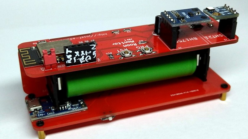
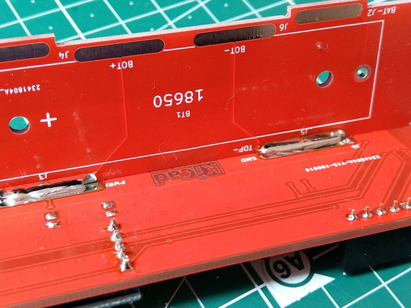
Which is how this ESP8266 sensor gadget from [Josef Adamčík] got its unique “folded over” look. The top panel is where the microcontroller and headers for various sensors live, the bottom panel is home to the TP4056 USB charging module, and the center panel provides mechanical support as well as holds the single 18650 cell. Rather than close the whole thing up with a fourth panel, he decided to leave it open so the battery can easily be removed. Plus, of course, it looks cooler this way.
 Could [Josef] have fit all his electronics on a single 100 x 100 PCB and then put the whole thing into a 3D printed enclosure? Well, sure. But that’s been done to death at this point, and besides, he was looking for an excuse to get more comfortable doing PCB design. We think it also makes for a considerably more visual appealing final product than simply taking the “normal” way out.
Currently [Josef] has an SHT21 humidity/temperature sensor and a BH1750 light sensor slotted into the headers on the top side of the device, but they could just as easily be swapped out with something else if you wanted to do something a bit more exciting. We notice that homebrew air quality monitors are becoming increasingly popular.
Building bespoke enclosures from PCBs is a fantastic trick that frankly we’d love to see more of. It’s somewhat of an artform in itself, but if you’re willing to put the effort in to do it right the results can be truly phenomenal.


Does Poland provide sufficient counseling for the mental health of their citizens? Seems like the winter is affecting this guy and this project is a cry for help.
really? Why?
Well, I am just afraid of those thiny-tiny traces used for battery line. If he has so much place, why not using proper traces?
200mA peak for ESP8266? Is there any real problem? Also – if things go wrong – they’ll work as a fuse :-p
You mean Czechia, right?
Hey, I am not sure about Poland since I am from Czech Republic an live in Germany ( I am “this guy”, BTW). I hated my counselors since they wanted me to paint pictures and coloring-books. So I stopped seeing them an started soldering. Works pretty well.
I like your project. Thanks for posting!
Sorry some people haven’t left their cave for a while.
Well, the guy is Czech working for German company thus we can presume he lives in one of those countries. He is young, employed, has a hobby and writes about it I’m not affraid about his mental health. More often the retired old folk with no hobbies – trolling doesn’t count as one – have mental issues during the dark and cold winters. But don’t despair – the spring is comming!
Ventilating the basement would work, too, and is available long before spring time ;)
What I would be interested in is creating the entire device from 1 PCB. Similar to how people are using a laser to create a “living hinge”
https://www.youtube.com/watch?v=JSlRusl7UPc
I’ve seen this before on an electronics exhibit in the Netherlands. Search for “Flexklok” on google. It was only the powertraces that traveled the bend but still was pretty cool. https://fhi.nl/eabeurs/gadget-2019/
I came here to caution about the chemical content of these boards and cutting several hundred through lines with a laser cutter sounds like a good reason to mention it. The material consists, usually, of fire retardants. If you’ve ever cut one, you know it takes a long while to get the taste out of your mouth and probably took a few years of your life with it.
Filed under mistakes not to make / repeat.
At best it is a 3D art/mess of PCB as there is no consistency. The components aren’t exactly ”enclosed” inside the space between the wall such that it would protect them.
It’s definitely neat, and not wanting to diss the hard work That’s gone into this, but it’s NOT an enclosure, as it doesn’t enclose the components, and crucially, the boards therefore don’t provide protection.
It’s an interesting dev board shape, and certainly more robust than some ESP & battery options I’ve seen. Those components on headers are very vulnerable.
If the components were on the inside of the shape, it’s probably reasonable protection, though I’d be slightly worried about the boards becoming disconnected if it was dropped?
I did a little ESP project and repurposed a USB power bank, fitting the ESP into the area the charge/5v circuit had fitted. There’s a lot of millage in those little cases, and they’re dirt cheap online.