There are a host of PCB CAD tools at the disposal of the electronic designer from entry-level to multi-thousand-dollar workstation software. It’s a field in which most of the players are commercial, and for the open-source devotee there have traditionally been only two choices. Both KiCad and gEDA are venerable packages with legions of devoted fans, but it is fair to say that they both present a steep learning curve for newcomers. There is however another contender in the world of open-source PCB CAD, in the form of the up-and-coming LibrePCB.
This GPL-licensed package has only been in development for a few years. LibrePCB brought out its first official release a little over a year ago, and now stands at version 0.1.3 with builds for GNU/Linux, Windows, MacOS, and FreeBSD. It’s time to download it and run it through its paces, to see whether it’s ready to serve its purpose.
Getting To Know LibrePCB
It’s refreshing to see for a project still early in its gestation, that the LibrePCB team have made an effort to provide a seamless installer rather than relying on a git command or a compressed archive. Installation on the Ubuntu system here was intuitive and easy, with selecting directories a straightforward process. When starting a test project, you’re required to set up libraries before it’s straight into the schematic editor, with as expected an easy flip between that and the layout editor.
The first impression of the interface is that it’s much simpler and more intuitive than its open-source competitors, as a former Eagle user who’s never found herself completely at ease with KiCAD I immediately felt at home. That learning curve I mentioned was largely absent, and though not everything is in quite the same place, the workflow and methods are similar enough to get started without any problems.
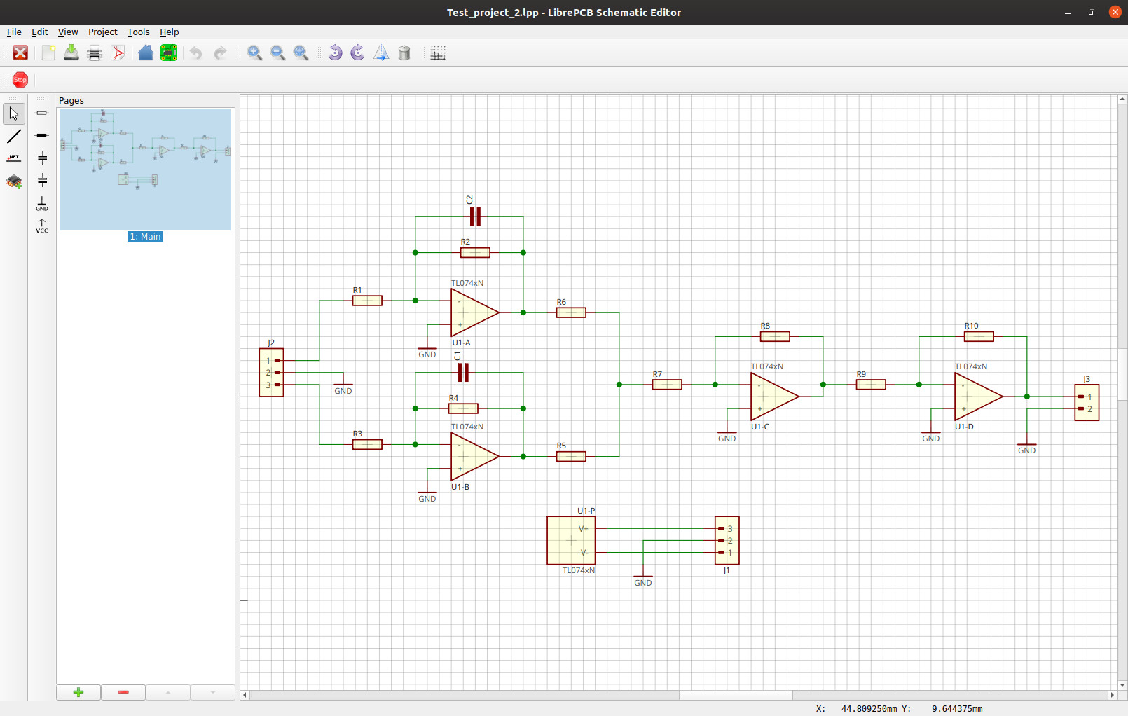
Without anything in particular to build, I set straight in to a simple multivibrator to put it through its paces, and then for something a little more complex an analogue mixer with a ground plane. Immediately a shortcoming of such a youthful piece of software fell into sharp relief, as it became obvious that the component libraries shipped with it were far from comprehensive and in many cases symbols lacked footprints. Not a problem, indeed it gave a convenient chance to take a look at the footprint and symbol editors to create a new component.
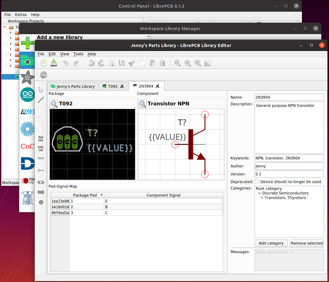
Call me old-fashioned, but my first simple test was a discrete 2N3904 transistor. It was a simple enough footprint to create but I found I couldn’t create the desired TO-92 circular outline due to the lack of ability to create an arc. I had to make do with a join-the-dots line, but I’ll take it. Maybe I should have arranged the pads in a triangle rather than a line, but LibrePCB lets you add alternative footprint easily enough. Instead of treating a package as a single footprint it can hold a variety of different footprints and types of the same component in a single one of its packages, so for instance for my TO-92 package could contain in-line, triangle, and ammopack versions.
A Few Rough Edges Still To Be Found
An unexpected issue showed itself as I created my component layout. I had selected one of LibrePCB’s stock SMD resistors in my schematic, but what showed up in the board was a through-hole component. Checking the stock component’s package in the component library revealed nothing but the SMD footprint in the component I had selected, but there it was. Creating a new SMD resistor component and substituting it for the stock model brought the correct footprint onto the board, but evidently I had stumbled upon one of the rough edges inherent to what is still an alpha piece of software.
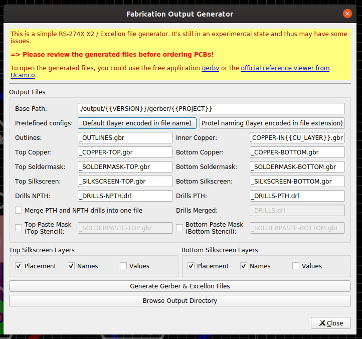
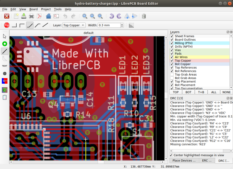
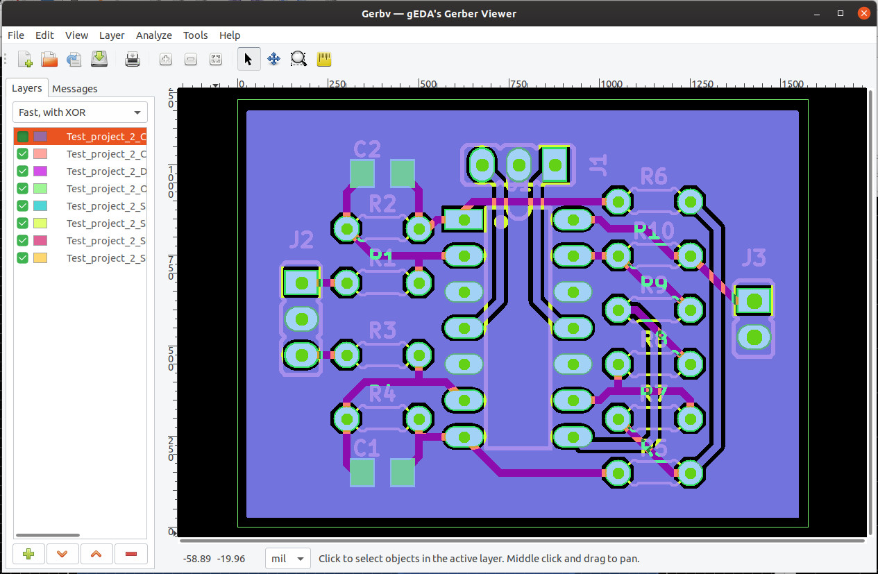
The point of a PCB CAD package though is to make PCBs, so next up was to run a design rule check and export my design. Writing this just as Chinese New Year is upon us there’s little point in ordering PCBs for a couple of projects I don’t want anyway, but I can still create a set of Gerbers and take a look at them in gerbv.
Design rule checking is a new feature in version 0.1.3 and an annoyance is that it doesn’t save any changes you make to the defaults, but it does warn you of this and lead you to expect that this will change. It would be nice to have the option to load and save different DRC settings to hold the various demands of different board houses. Gerber export is extremely straightforward though, and I soon had a set of files that loaded up with a board that appeared exactly as I expected in gerbv. I have no reason to believe that if I sent them to a board house I wouldn’t shortly receive a set of PCBs without queries about the quality of what I had sent.
Is It Ready For The Big Time?
It’s quite possible then to use LibrePCB as it stands to design a simple PCB and create the Gerbers for a board house. You can certainly give that a go, but while they’ve made a commendable achievement of a remarkably usable piece of software for one at such an early-stage in its life it’s still one that has a little way to go. There will be a few bugs, it’s evident that there are features still to be implemented in future versions, and the stock libraries are hardly comprehensive. Both of the first two will inevitably improve with subsequent releases, and the last will grow as the user base expands.
Whenever a new open-source project arrives that does the same task as an established software libre player there are inevitably voices that decry it, as though somehow it is diluting the available resources for its competitor. I don’t agree with this view as I see diversity as essential to the ecosystem, but it’s worth asking what LibrePCB will achieve and where it will find a niche.
Perhaps the answer to that question will satisfy those worried it might take resources from the likes of KiCAD then, because after using it I feel its strengths lie in a completely different direction. A few years ago the default in our circles was Eagle, but the sale of that package to Autodesk and subsequent move to a subscription model has weakened that hold. LibrePCB is unlikely to tempt the professional Altium user or the established KiCAD user, but its ease of user interface migration for long-time Eagle users gives it an opening that KiCAD struggles with. If they can enhance that experience and provide a migration path for Eagle projects in both old and new formats I think they’ll be on to a winner, and could easily become a regular sight in projects we feature here.
So, should you install LibrePCB? By all means, install it, get to know it, and contribute to it if you have the relevant skills. Should you use it to design PCBs? You certainly can and there’s no harm in trying, but you’ll inevitably run into one of the limitations in the current version due to its early-stage status. Should you abandon your other tools and make the move to the current version of LibrePCB for all your work? Probably not, unless you like to live dangerously. I think LibrePCB is one to watch, they’ve done a very good job so far and I think there is a possibility for an extremely useful piece of software from it in the future. Watch that space.


I tried a pre-1.0 version of LibrePCB a year or so ago. As a long-time Eagle user, I was able to go from installation to well-formed gerbers for a simple SMT layout in under 10 minutes, without reading any documentation.
Although several advanced features were missing at the time, I’d say the UI seemed like a polished and friendly (and long-overdue) Eagle rewrite. Under the hood there seem to be a lot of good architectural decisions, and ongoing efforts to incorporate great open source components like KiCad’s push and shove router.
Urban Bruhin and collaborators have done some truly impressive work, and I’m excited to see where it leads.
Wait a few years until this package has feature parity with kicad an gEDA. Than we will see if it still has that “low” learning curve. Also the the learning curve for kicad is not that bad. Compared to eagle they just expect you to now more keyboard commands.
Coming from protel99 I found eagle unbearably counterintuitive. KICAD was a breeze, felt at home in 5 minutes…
KiCAD is the way to go anyway, EAGLE is autodesk property and therefore anything designed in it is theirs as well.
I can tell you that if I had to choose between KiCad, and anything coming from Mentor, I’d happily choose KiCad.
Due to how bad and unstable PADS used to be, Mentor Graphics is called Mental Hraphics where I work.
I’m frankly surprised about the comments about the KiCad learning curve.
As a complete PCB beginner, I went from downloading KiCad to submitting a Gerber for production in one evening.
Maybe past experience of Eagle with different use patterns results in a more difficult transition to KiCad?
For me, the main frustration with gEDA and KiCAD both has been new part creation (specifically, making pads in gEDA, which is a throwback to how gerbers are coded, and in KiCAD getting newly created parts to show up in libraries.) I think maybe this is just a hard project, because the best layout tool I’ve gotten to use, Cadence Allegro, has an appalling library management system. If there are people out there designing The Next Big Thing in opensource layout, see if you can figure out a good way to do a padstack -> footprint -> logical pin to physical pin mapping -> symbol and footprint library update process. Altium does pretty well at this. OrCAD did okay too. After reading this, I’ll try out librepcb tonight, and have high hopes it’ll do a good job.
Also, if you want adoption, this may be obvious, but making tools that allow import of libraries from other packages goes a very long ways. Cadence Allegro is even capable, to some extent, of importing full pcb’s from other layout packages, which was an enormous help sometimes.
I used to use a (now extinct) package called ProCad that allowed you to sketch the symbol in the schematic capture window or the layout window, putting down primitives for the pins, etc, then you could select the picture you just drew from from lines and arcs and text *on your schematic* and bring that into the part editor where you could add pin information, etc and make a real component.
I will freely admit that I have not tried all the schematic packages, but I have yet to find this function on the other ones I have tried. I miss it, it was fast, often you just grabbed an existing part, smashed it, changed a couple of things, and resaved a new part, and the part was always the right size and shape because I could draw it in-situ.
I think that you have that functionality in Proteus (from Labcenter).
If you haven’t edited footprints in Kicad for a while, I’d suggest you give it another shot. Back in 2015(-ish!) I really struggled with Kicad. Even when i followed up-to-date tutorials and videos, I’d still get stuck, or fail to find where/if my footprint had saved, or had drama reusing the footprint in new projects (I am pretty sure my fp-lib-table etc were correct, but damn that system was opaque!) This was with both windows and linux mint.
Fast forward to 2019/20 and making my own footprints seems to “just work” in Kicad now. I don’t need instructions, just click on the footprint editor. Save the footprint wherever I want, and there it is waiting to be dropped on a PCB. The Kicad team seemed to really listen to users’ feedback and have really improved the users’ workflow here.
I’m not in front of a computer to check the version I’m using, all I can say is it’s some recent, stable build from the official repo (I have now mostly switched to linux and ditched windows almost entirely)
I used Eagle for a few years before migrating to Kicad. All I can say a few years later is that I am very glad I took the plunge and moved away.
Hmmm might be worth a shot at getting into Kicad again then. My big thing in pretty much all of this type of software was that my parts were never in the damn library. Given that I rarely ever want to do anything that can’t be sketched in 3 minutes on the back of a small envelope, and that I’d have it soldered up on stripboard before I’d have even got just the OC44 or tin cased 741 halfway done in the part editor. If ever I needed to break out a crisp sheet of A4/Letter sized paper to do something bigger, I’d suck up the extra 2 hours it’d take me with pencil and eraser, thinking it would take 30 minutes per component for the 20 components out of 40 that probably weren’t going to be in there.
Does KiCAD still force you to choose between two partly-working display drivers, or has that finally been finalized into one solid, fast, working thing ?
I think what Michael Brenden is referring to is Kicad’s option to use accelerated graphics or software rendering. Both work for me, under both Windows and Linux. Sorry it didn’t work for him.
This is why I felt in love with Diptrace. Creating new parts is really easy and straight forward. Made a ton PCB with Diptrace, works quite well.
All the rest? They could rule the world. If they would bring the GUI into 2015… If they rework the parts management and parts search (like in LibrePCB, great job!). If they add easy access to parts distributors and automatic pulling parts from their web sites. If they hear their users and add all the small feature requests and do the mini bug fixes.
One simple addition could be nice, a simple type of component, smd or through hole. When selecting footprints, have a 3 way drop down, both, smd or through hole, that would simplify the selection by only showing the relevant option. As this is a production preference, it should be pretty constant for the selected board.
Kicad learning curve is not that steep.
It only looks steep for long term Eagle users that so far have almost forgot how tough was to migrate from Tango, Circad, etc…
I took the Kicad road a long ago and now Kicad and Eagle are equally easy to use and my perception is that the learning curve from both were equivalent.
Nevertheless,g LibreCAD is very welcome!
Pretty sure KiCAD I objectively way harder to use. It’s heavily reliant on unlabeled keyboard shortcuts, and it’s also not really an integrated package.
You almost always wind up with dozens of subtle annoyances when you do GUI software as multiple separate programs loosely glued together. It was really popular in the UNIX philosophy days, but most new stuff that catches on and takes over seems to be highly integrated, and for a reason.
Last I checked, the only way to get Eagle now is to subscribe to Fusion 360. Autodesk has finally put the nail in Eagle’s coffin. When I first started designing PCBs, I tried many cheap/free tools, but they were tied to a particular boardhouse. I finally settled on Eagle since it was affordable and I was paying out of my own pocket. Librecad is something I will look into.
Eagle 6.3 very much still works. There’s no reason to believe PCB technology will be changing in a way that would break it any time soon, either.
KiCAD is fine. Maybe this new tool is too… but Eagle 6 made it easy to make _pretty_ PCBs. It’s still indispensable for quick projects where you care about that.
I’ve completely given up on waiting for KiCad/gEDA to fix their UI. Blender did, so anything is possible, but… this will probably get there first.
I think LibrePCB will be the CAD of the future, assuming they do things right and leave the door open for all the high end advanced stuff like constraints.
At the moment I haven’t seen any issues that would make me hesitate to use it for most basic hobby type things, aside from the fact that it really needs to be able import from at least one of snapEDA’s export formats.
Not that it matters that much, Libre already has the best part creation I’ve ever seen(Points editing for polygons would be nice, but meh).
Nobody mentioned EasyEDA. I’ve been using it for years and love it.
Seriously? EasyEDA is a horror show, PCBs created with it can be easily spotted from the other end of a large room.
Perhaps some HaD readers do not know, other than the initial cost, why some independents use KiCad -> scripting. I review clients’ designs using several sequential Python scripts; that is, DRC for both component values and circuit layouts. I had done this using mostly built-in tools at a previous employer with Altium stuff, but had to use other stuff when I went independent. And had to go 100% KiCad after two consecutive jobs where client company used Eagle – what a freaking mess.
I have donated to the KiCad project in monies and scripts in the hope that they would fix the component edit process. So will now sit and watch the LibrePCB project to see if it merits my time and dollars.
> So will now sit and watch the LibrePCB project to see if it merits my time and dollars.
While I understand that your time is limited, you could also chime in on the forum or the chat (https://librepcb.org/discuss/) and bring your experience with CAD software on the table to help shape the future of LibrePCB :)
What do people mean when they talk about a steep learning curve with KiCAD?
I used Eagle a lot in the 90s, up to 2004. Later, I used Altium at work. THAT is a steep learning curve. It might be great for use in big companies with a dedicated group administrating the parts library and databases. But for small project teams without external support it is terribly complicated.
Around 2013 I needed a (not too complicated) PCB again and there was no Altium available: So I used Eagle again, after a ten year break. And I gave up after two days of trying. Everything was so complicated. At that pace it would have taken two weeks to finish the PCB.
So I tried KiCAD. Using it for the very first time I felt at home right away. Three hours after installation I already got further than the Eagle experiment after two days. And the next day I was done and the PCB came out great.
To me KiCAD feels like a perfectly scaled down version of Altium: It offers the great features and leaves out the extras that are only useful for big project teams and require a lot of supporting work in the background. The only feature I start to miss is the possibility to define different sets of output operations: Layer configurations, DRC parameters, file name conventions etc.
This would be excellent with a simple add-on such as pcd-gcode is added for my basic pcb making. I like the simplicity and similarity to eagle. kicad has too many quirks to learn basic placement and component selection. Particularly when i want to make a library of common use components and do not need to learn and memorize the variety of packages. I do this as a hobby, not a job. Thank you for sharing Jenny.
But what if you confuse a TO-92 with a T-34 and find you’ve made a tank circuit instead of a filter?
I should probably avoid electronic circuits if that were the case. https://en.wikipedia.org/wiki/T-34_variants
Urban Bruhin and other contributors put incredible amount of effort to that tool already and I am very glad that they choose the right toolkit (Qt) for the project.
I wanted to contribute to the code so I started to build it on my notebook and it went to thermal shutdown after 10 minutes of compilation with 8 threads. Of course it was a notification about the fact that the thermal system needs cleaning, however it shows the amount of the code they built already.
> Urban Bruhin and other contributors put incredible amount of effort to that tool already and I am very glad that they choose the right toolkit (Qt) for the project.
Your comment is very funny in context, since the choice of the “right toolkit” is exactly why your poor notebook went nuclear. Using one of the many of the “wrong” toolkits most likely wouldn’t have been an issue at all since Qt is an utter CPU and memory hog.
you didn’t even read the comment you are commenting on, his computer overheated during compilation, Qt has nothing to do with it. PS sorry about your nervous knee jerk
> Using one of the many of the “wrong” toolkits most likely wouldn’t have been an issue at all since Qt is an utter CPU and memory hog.
Your comment looks even more funny from my viewpoint. Qt was ported to STM32 and other MCU series recently and having been used in many memory and CPU constrained embedded application.
Anyhow not the development frameworks making applications memory and CPU hog but the practices what the developers apply during the development, and the overall features which got implemented.
But when it comes to open source contribution (at least for me) it is very important that the project uses a framework which has good documentation, proper IDE support, etc.
>But when it comes to open source contribution (at least for me) it is very important that the project uses a framework which has good documentation, proper IDE support, etc.
You seem to confuse Qt for GTK
I have a very different definition of CPU hog than you…. Qt is blazing fast, like any native C++ toolkit for the most part.
If you tried to reimplement all the extra stuff Qt does yourself, you’d probably wind up with just as much CPU usage. If you just leave it out, you wind up with an unpolished mediocre app.
It’s July 2049, year 50 of the toolkit wars. All is ashes.
The Qt armada were crushed by the adherents of GTK, but were routed by a sneak attack by the WX brigade. In their desperation, the Motif clan detonated their doomsday device. Now Swing rules the wasteland.
Beyond hand-drawing a layout, transferring to a copper-clad board and a ferric-chloride bath, and breaking a succession of tiny drillbits (… many years ago), I have not done any PCB layout recently. It seems I can get something working fast enough using stripboard or Manhattan-style construction, and there was no point to investing the time into learning a complex a demanding PCB design software.
Am I right in thinking that LibrePCB might be a faster and easier way for the PCB n00b to design some basic and non-critical boards?
Give it a try!
As a beginner, I did my first PCB less than a year ago with KiCad and it was easy and fun. (https://tomverbeure.github.io/2019/02/05/VGA-I2C-My-First-PCB.html)
Now, I often just don’t bother breadboarding or soldering prototypes anymore: I fire up KiCad, send out a board the same day, and switch to a different project while I wait for the PCBs to arrive.
Amazing how cheap things have become.
Even if I am doing my old projects, I spend my time and use schematic/PCB. I can make another copy or a dozen copies of a working project easily. The layout contains a lot of info of what parts go where and is useful for repairing.
Hand drawn schematic can get misplaced over time and not as easy to share.
I’m surprised that the author complained about Kicad having a steep learning curve. It’s actually quite intuitive. It’s power full enough that they n a conversation with a head marketing person for Altium, they lamented the existence of Kicad. As a Post Doc Researcher at UNSW , I prefer using Kicad over Altium and so does my colleague.
The features that nail it for me are being able to draw up subcircuits within a circuit layout and then drill down. Super powerful. Also you can pull the parts and PCB layout as STL file and export it to a 3D package. I use that to fit and connect Arduino PCBs to extension PCBs. Then I build the casing around these in 3D. The power to be able to export into a 3D package (I use SolidEdge) cannot be underestimated. Once you try this, you’ll never go back to old ways.
I applause new work on Libre but for getting work out the door, I’ve found Kicad is solid, mature and dependable.
Please excuse typos on my original post. The auto correct on my cell phone plays havoc with the text and there is no way to re edit the text and fix typos.
As a contributor to LibrePCB: Thanks for this very nice and very fair review :)
One thing I wanted to note though: It’s already possible to use arcs in polygons, but right now you have to double-click the polygon and manually enter an angle (in degrees) for one or more points. A GUI for editing the polygon in real-time will surely follow in a future version!
I recently went from Eagle to KiCad and found it quite easy to change. It is odd though as I tried a number of years ago and it was near impossible for me to change. Has something happened with the interface with KiCad recently? Or have I changed and picked it up easier?
The feature I miss… and I don’t know if any EDA has this (I’ve used gEDA and KiCAD).
I’d like to be able to design a sub-module (e.g. maybe an analogue filter, or maybe a MCU and its supporting hardware), create a PCB layout for it… then in another project, import that other project as a component with its own footprint.
Thus, inside the schematic for the “superproject”, instances of the “subproject” would appear as a “black box” components and in PCB layout, you’d just place “copies” of the subproject’s laid out PCB, before drawing wires and other connections between them and the rest of your circuit.
Not sure how designations would be handled, maybe they just get prefixed,or it could be they get mapped and re-numbered so they flow naturally in the parent schematic.
Doing this would save a lot of time. You could design your sub-circuits once, and literally re-use them like you do for components now.
Nice idea, I added a thread in the discussion forum for this: https://librepcb.discourse.group/t/subcircuits/192
Heh, save time you say. I’d go off into the woods designing endless modules and never get round to actually putting any together in a project.
Altium does this with snippets or “convert sheet to symbol”
This! And KiCAD is basically begging for this workflow with the heirarchical sheets, IMO. You can already pull in a “module” into a schematic with a defined set of ins/outs. All that’s missing is the PCB layout step.
There’s a really useful plugin for Kicad that allows duplication of layout between hierarchical sheets: https://github.com/MitjaNemec/Kicad_action_plugins#replicate-layout – it worked perfectly on my first attempt with it (and eight-channel MIDI to CV board).
Oh wow. That looks really good. Will have to give it a try.
Action plugins may be the best thing to happen to KiCad since push & shove.
I wish ORCAD was still around.
Perhaps not totally on-topic here but ORCAD was the reason I used TinyCAD and FreePCB (both free) for experimental boards at work and still for my own designs after retiring. At work they decided to transition to Altium which I also found to be less than intuitive. Glad I don’t have to use either ORCAD or ALTIUM now.
I have also tried Eagle and KiCad but not impressed.
Orcad has changed a lot now. New Gui, new pcb features water falled from allegro an plenty of leeway to do more powerful things.
tools like Z depth for vias, static and dynamic phase adjustment, new solid edge 3d engine has been grafted in, new pad stack designer, new constraint management from schematic through to layout. I used to use Labcentres proteus but now for complex board up to 18 layers with complex constraints I actually having tried pads and altium prefer Orcad. It has issues you pull your hair over or take multiple steps to do but all tools have this. Altium is more polished but is slow on a low power machine in pcb or 3d. Orcad is much faster. clash detect of enclosures, graphical stackup management rather than text file editing, easy revision up and down the netlist to and from PCB, slowly Cadence are addressing many issues in Orcad and with EMA add on tools and the CIS library management its very good. th eSI simulation basics and PSPICS now too (in 17.4) are free. I tried altium recently and found much to be complicated or counter intuitive after several years of not using any tools. Im sure its a great tool but my Im getting too old to fight the tools. Agreed on KiCad. It is a very good tool.
The biggest issue with all the EDA tools on the market is they all violently suck! The user interfaces were designed by people who have no concept of how to design a proper user interface. Every single schematic editor screws it up. Yet, every new application continues to follow the same old asinine UI convention.
A well designed UI shouldn’t lock the user into a “mode of operation.” You should be able to perform any operation without having to explicitly cancel and an existing operation. Want to wire two pins together? Click on the source pin and while holding down the mouse button, drag out the wire to the destination pin, and release the mouse button. Want to abort the operation? Just release the mouse button anywhere where there isn’t a target.
These conventions are not new. They’ve been around since the birth of the GUI.