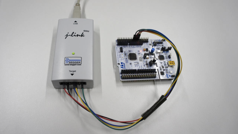
In a perfect world, everything would be open source. Our current world, on the other hand, has a lot of malicious actors and people willing to exploit trade secrets if given the opportunity, so chip manufacturers take a lot of measures to protect their customers’ products’ firmware. These methods aren’t perfect, though, as [zapb] shows while taking a deeper look into an STM microcontroller.
The STM32F0 and F1 chips rely on various methods of protecting their firmware. The F0 has its debug interface permanently switched off, but the F1 still allows users access to this interface. It uses flash memory read-out protection instead, which has its own set of vulnerabilities. By generating exceptions and exploiting the intended functions of the chip during those exceptions, memory values can be read out of the processor despite the memory read-out protection.
This is a very detailed breakdown of this specific attack on theses controllers, but it isn’t “perfect”. It requires physical access to the debug interface, plus [zapb] was only able to extract about 94% of the internal memory. That being said, while it would be in STM’s best interests to fix the issue, it’s not the worst attack we’ve ever seen on a piece of hardware.


I’m wondering why STM did not respond until https://www.cert-bund.de/ was involved? That sounds odd.
99.99% of the time these companies ignore any and every email which is not from the domain of another huge or already known company (customer).
Well, first and foremost, people at ST have probably a lot of work to do on the new chip. So, obviously some time could be used to correct some bugs, but they will not have a lot of time too.
Second, the bug find here is at a hardware level if I understand correctly, so it will involve redesigning part of the chip to the waffer level, test it, and verify that there is no regression. Again, it takes a lot of time and money to create the new waffers (not as easy as a git push).
Lastly, I think that a big company like this is better off to say nothing, correct it, and then silently pushing a new chip revision than screaming out loud that they goof up and will correct it asap. It will prevent further spread of the attack, and the patch can be a “surprise” to the hacker community.
Personally, I both think that people should be able to reprogram the chip and that if company don’t want to give their code, they should be able too (but should give all the opportunity to reprogram the chip, like, not using OTP chip, and give access to programming pins). New laws goes in this direction, but then, some will find a way to go around I think…
The F0 series have a similar thing going on: https://www.aisec.fraunhofer.de/en/FirmwareProtection.html
You can disable the swd/jtag by setting some bits in the alternate function register.
I did this once and could get it to work again.. I lack the skillset of these guys so I think it isn’t as safe as I assume it is :D
The usual way of recovering from this is holding NRST pin low while connecting.
For me using a supply voltage glitch worked well in tricking the built-in-Bootloader of a STM32F103 into executing the “memory read” command despite the lock bit being set. I found this possibility in the Paper “Shaping the Glitch: Optimizing Voltage Fault Injection Attacks” and adapted it for me. Used it to repair a defective Roomba 980 by replacing the main STM32.
Playing with voltage was also a technique used to crack the “secure” vm of the Xbox360 if I remember. There was a talk at the CCC years ago about that, if I manage to find back the link…
An interesting article, but it would be even more intersting to see ow complete the extraction is graphically. It looks like they miss chunks of data in repeating patterns, so one way atound this might be to store your secrets in the non-readable parts,even if this makes the code layout and setup more complicated.
Since I’m a newbie and have only played a little with STM8 parts, the question I have is can you upload new firmware without wiping all the existing flash? I suspect not… but maybe you can somehow?
STM8 is the only oddball I have seen that doesn’t require an erase before writing arbitrary bytes to FLASH. It is more like EEPROM with a memory bridge that hides the actual programming such that it behaves like RAM.
In another word, the programmer software only need to overwrite the actual bytes used in the new firmware. It might decide to zero the unused bytes depending if you want a full chip “erase”.
(I hope this comment lands at the correct place as an answer to zoobab[1])
I seem to recall something similar but can’t find the video either…
… unless it is this one: https://media.ccc.de/v/27c3-4087-en-console_hacking_2010#t=1128
[1] https://hackaday.com/2020/03/24/breaking-into-a-secure-facility-stm32-flash/#comment-6230887
Grab supervisor mode by holding nRST low during boot, boot in DFU mode using i2C / SWD, and when the chip reads the RBP fuse (this can take timing experimentation), glitch the power rail… insert dumper code in 0x24000000, and jump in, reading your ill-gotten code from the peripheral you chose for the dump. ST hasn’t changed since the ST19NA18 Smartcard.
Rookie here..
What does it mean that the swd/jtag is disabled on the F0? I have a cheapy discovery board that I’ve debug with presumably via swd, what part is disabled?
Are ST’s security measures meant to prevent reading the flash that the user programmed (not ST’s bootloader ROM section)? But I’ve seen people implement custom bootloaders, don’t these read and write to the flash memory?
A copyright/”security” protection feature by programming a special “fuse” that can disable hardware debugger.
And how about the F103 clones that circulate around, it would be great to see how they cope with this method.
See https://blog.zapb.de/one-exploit-to-rule-them-all
Help me out here, I’m not familiar with the F1 series. I only ever worked with F4, L4, F7 and H7.
The F446xx hast RDP level 0, 1 and 2.
Is the article talking about RDP 1 or RDP 2? Does the F1 only have RDP 1?
i found the posted code not working, being a python id10t i could not fix it but did find someone who had, https://github.com/doegox/stm32f1-firmware-extractor and it does work.
The Python code is working but requires a recent version of OpenOCD.
I tried with latest OpenOCD and python 2.x – 3.x and the original pythong code still fails , the deogox version however has the fixes to work with older OpenOCD and both main python versions.