The idea of trying to prototype with SMD parts on the fly sounds like insanity, right? But then we watched [Leo Fernekes] walk calmly and carefully through his process (video, embedded below). Suddenly, SMD prototyping jumped onto our list of things to try soon.
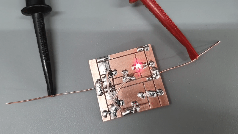
[Leo] speaks from a lot of experience and tight client timelines, so this video is a fourteen-minute masterclass in using copper-clad board as a Manhattan-style scratch pad. He starts by making a renewable tool for scraping away copper by grinding down and shaping an old X-Acto blade into a kind of sharpened Swiss Army knife bottle opener shape. That alone is mind-blowing, but [Leo] keeps on going.
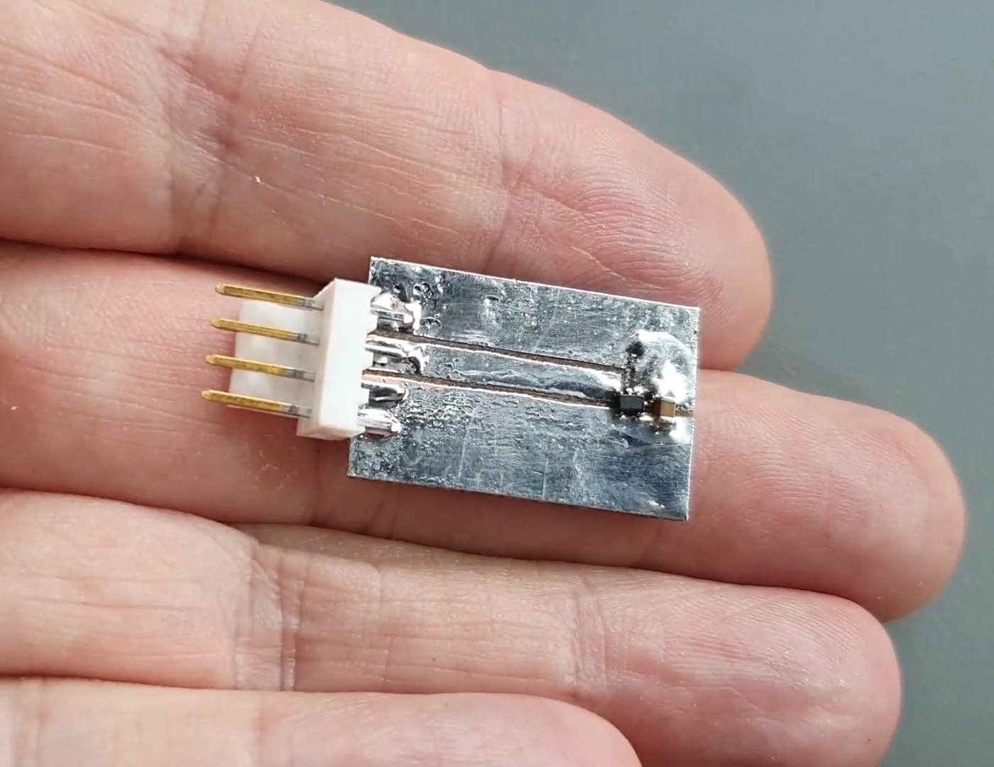 In these prototypes, he uses the through-hole version of whatever microcontroller is in the design. For everything else, he uses the exact SMT part that will end up on the PCB that someone else is busy designing in the meantime.
After laying the board out on paper, [Leo] carves out the islands of conductivity, beep-checks them for shorts, shines the whole thing with steel wool, and goes to town.
The tips and tricks keep coming as he makes jumps and joins ground planes with bare copper wire insulated with heat-proof Teflon tubing, and lays out the benefits of building up a stash of connectors and shelling out the money for a good crimp tool.
And why do you need a good crimp tool? Because when they’re done properly, crimped connections are stronger and more reliable than solder. There’s a lot more to them than you might think.


The tool is convenient, but the cut seems rather wide, so it wouldn’t work well with fine pitch stuff, especially not if it has more than 3 or 4 leads.
And the MCP9700 he used as an example is also available in SOT23, or even through hole. Why not use that one instead ?
His entire point is to use and validate the part that is going onto the final board, not just the one that is convenient for prototyping. Obviously this won’t work for super-dense parts but that’s why he also recommended having surf boards on hand to break those out.
Yeah, I got that, but I see no reason to think that the SOT23 version of (a lousy) temperature sensor is going to behave different than the SC70 version. I’m pretty sure that the actual silicon inside the different packages is identical.
Any small difference in thermal characteristics of the package will be completely overwhelmed by differences between his proto board and the final product, or even between different production runs of the silicon.
The tooltip widh shouldn’t be too hard to adjust if you have a to grind it anyway?
If the package was important enough that you would want to proto with the actual design package then I fear the PCB layout will be just as important and this approach obviously uses a layout that is not final.
Rapid two layer PCBs are cheap and will yield better results in most cases.
There is a place for this type of prototype but I don’t think it should be part of many design cycles.
Very good video, has some high value tips in it!
I agree with everything EXCEPT the recommendation to get the official Molex crimping tool, no need for this, a medium priced (30€) work too! I have both, and use the Aliexpress version more often as it’s lighter and easier to handle. Just make sure to get a ratchet model with perfect anvil/punch cut, not cheap stamped steel. (actually I even have 2 of theses Chinese model, one for adjusted for thin wires and another one for thicker or doubled wires)
Yeah, I did a double take at that. I generally agree that it’s worth spending a bit more for decent tools… but “official” crimp tool prices are just insane. For the type of JST connector I use, I think the official hand tool is something like $700, and it’s not like that will even make the work faster.
I just use a pliers-style crimper (an Engineer PA-09), with the advantage / disadvantage that you can control the crimping force by sight and feel. It may not produce NASA-standard connectors, but I definitely haven’t had $680 worth of problems.
That said, you should probably check how much the OEM tool actually costs for your connector type, because the prices vary wildly. If it’s only $50 or even $100 then you should probably listen to this guy’s advice rather than mine.
I crimp a LOT. I think ratchet crimps are totally worth the money. Maybe not molex: there are aftermarket copies. But it’s been my experience that no matter how good a job I think I’m doing with pressure on a hand crimper, a ratchet crimper does a far better job as evidenced by the longevity/durability of the wire harnesses we’ve built.
Plus they’re a whole lot faster when you’re doing double crimps, wire/insulation. More than 2x as fast, so after 10 or so crimps I feel like I’ve repaid the extra cost of an inexpensive ratchet crimper.
Doubly the case on automotive wiring harnesses. Quinn Dunki pointed out an automotive quick disconnect crimp tool one time, I got one, and I haven’t even looked at my old about-like-that crimpers since.
I always ask my students “which wire connection can we afford to fail?” that quiets them down pretty quick when they look at the nest of wires they just created. I have a big collection of painfully expensive crimpers – it’s actually cheap insurance in the long run if you value your reputation.
Good crimping tools are worth it. The smaller the connectors, the more critical the die dimensions are. Especially when you’re crimping a few hundred terminals for a product that needs to work.
There is a lot of instances where the hacky techniques in scratch boarding are quick, but at the same time, that clad board can almost as quickly be used to CNC engrave, depending on your personal workflow. Not to mention, there’s added capacitance to be accounted for, when you have vast surfaces of copper… love it all definitely. These are still killer tips to keep in the toolbox.
It’s great for apartment buildings though, where you can’t have a wailing desktop CNC machine for the sound, and for the glass fiber dust it puts out.
good find!
Have open to watch later. Reminds me I need to grind/file down the point on the hole punch tool for those style riser fab.
Looks like an interesting watch with great detail.
An exacto ground the way indicated is very awkward to hold. In the jewelry trade they use a ‘graver’. Generally used with a palm handle. They’re only a few dollars. Much easier to hold and control than an exacto. I have an assortment in different widths from hairline to 100 mils or better. You can get the usual HSS which needs to be sharpened fairly often (easy using a Dremel or a stone). Or, you can get carbide which holds an edge much longer but needs a diamond stone or wheel to sharpen. Use a small wood block with a little ledge to hold your board and avoid stabbing yourself 100 times. Use carbon paper (What’s that?!!) to transfer lines onto the board. Or, draw with a sharpie.
Beware of double-sided PCB. There’s typically 17 pF per square inch or 1.5 pF capacitance for a 250 mil square pad. You need to factor that into the circuit design and remove copper from the back (usually ground) where necessary. You can do vias to the back side and avoid flying jumpers. With care it’s possible to lift a corner of a large copper area and peel away the copper to remove larger areas. Faster and neater than scrubbing it off with a graver. I’ve been doing breadboards this way for many decades.
Heat gun makes removing the back side copper about 20x easier. I use a hot air pencil. It peels off like a sticker on a banana.
If you use a heavy xacto to put an incised line on the copper, you can then follow the line with the graver a lot more easily. I’d like something that’d cut two lines about 0.2mm apart because then I could peel off the 0.2mm and have a nice wide separation.
At work I use an LPKF board plotter, and set the insulation width depending on the voltage, and peel off the intervening copper (or all the no-net copper, if capacitance is a problem) with a hot air pencil. The boards come out quite nicely, and it’s really helpful to our design people that we can go through four different board layouts/revisions per day until they get the one they like, and then we turn that one into a green board that’ll show up three days later. Sometimes we go through 10 or 20 revisions in that first few days, though.
The heat trick also works well if you want to remove some pads of a proto board. Just put the iron on to heat the pad, and peel it off with the knife.
That’s a cool technique; I have used it a couple ot times to build video game prototype cartridges. And thanks the author for producing and sharing the video.
Personally I prefer to use Chan’s method with enamelled wire.
http://elm-chan.org/docs/wire/wiring_e.html
https://cdn.instructables.com/F5K/WU8U/H67NSJA9/F5KWU8UH67NSJA9.LARGE.jpg
…or don’t have the space available.
i needed some small boards, but rather than wasting an entire $2 blue sheet on two small boards (like less than a square inch). so i broke out the diamond file kit and freehanded it much like this. i think the best takeaway here is the tool he created which is a lot cleaner than the triangular diamond file i usually use. im gonna go make one right now.
Ah yeah, that’s one thing I’ve used, the ends of needle files. I’ve been trying to remember my “preferred tool” for this, but it seems like I use something different every time, since I don’t do it very often. Another couple of things are, broken hacksaw blades, holding so the teeth rake toward you and the last tooth on the end is more or less the same shape as his edge there. Then I’ve used drywall screws, which are always harder steel and stay pointy. Lately however, I’ve owned a dental pick with a reverse spadey end on it, and I score with whatever HD craft knife is at hand, or penknife, then rake it out with that. I’ve probably abused the pointy ends of scissors and side cutters at some time also.
Drywall screws are probably pretty easy for the “no shop no worries” crowd to make a “circuit adze”* just get 4 to 6 inches of 3/4 to 1 1/4 round or square or whatever softwood or dowel or wooden broom handle and drive a drywall screw through it at an angle, near, but not too near the end, leaned toward the rest of the handle. (Make a number 7)
* or make up an even fancier name for it, a discontinuity furrow insertion tool.
* Here are a bunch of Manhattan Style construction tips not mentioned in the YouTube video:
——–
* Ready made scoring tools
* OLFA 1090486 PC-L Plastic/Laminate Scorer Amazon’s Choice for “plexiglass cutter” $13.45
https://www.amazon.com/dp/B003UHUZ5U
* OLFA 5014 PB-800 Plastic/Laminate Blades, 3-Pack $8.08
https://www.amazon.com/OLFA-5014-PB-800-Plastic-Laminate/dp/B000BNLJ38
* YouU 1 Acrylic Cutter and 10 Pcs Blade Set, Multi-Use Cutter with Cutting Blade Brand: YouU $9.69
https://www.amazon.com/dp/B07S75XBYS
——–
* Isolated Pad Cutters
* Vector Electronics Pad Cutters
https://www.vectorelect.com/pad-cutters.html
* Cutting Islands Into Copper-clad PCBs With A Drill
https://hackaday.com/2012/07/20/cutting-islands-into-copper-clad-pcbs-with-a-drill/
* Circuit board ‘Land’ cutter.
https://www.youtube.com/watch?v=RKdsXU5iIF0
* PCB Tip, tip for creating pads on continuously coated PCB’s
https://www.youtube.com/watch?v=uFLdDTT5-wk&feature=relmfu
——–
* Cut PCB Isolated Pads
What you do here is cut a piece of solid copper-clad PCB (can be 1 or 2-sided) into pads – squares, rectangles, any size depending on your circuit layout using any method (hint: a nibbling tool can be useful, especially for small pads), then you glue the cut out pieces (copper side up) onto the surface of another piece of solid copper-clad PCB (can be 1 or 2-sided, with copper side up). This larger solid copper-clad PCB acts as a ground plane. Some prefer to use double-sided tape (not the foam kind) instead of glue, this allows the pads to be lifted and moved, and when the prototyping is done all (or some) of the pads may be removed so the base copper-clad PCB can be reused. Usually the builder will cut a bunch of small square pads, these are useful for small components that connect to ground and jumper pads where more than one wire connect. These small pads can be bought pre-cut, one commercial example is called MeSquares (see below) which includes a range of stick-down SMT component adapters.
* Here are a couple of examples of what this construction style looks like:
https://hackaday.com/wp-content/uploads/2016/05/original.jpg
https://hackaday.com/wp-content/uploads/2016/05/0gfwt.jpg
* MeSquares Pre-Cut Isolated Pads and SMT Stick-Down Adapters
http://qrpme.com/?p=product&id=SAM
* Here’s an example of a nibbling tool which can be useful for cutting out isolated pads:
* Parts Express Nickel Plated Nibbling Tool $13.28
https://www.amazon.com/Parts-Express-Nickel-Plated-Nibbling/dp/B0002KRACO
——–
Those Vector pad cutters: sooo sexy. Would be good for working with stripboard too.
Thin copper tape, if it’s got an insulating backing. Cut out little squares, stick them on raw PCB. Solder, done.
Or buy the scissor-cut epoxy PCB material that they use for multilayer board buildups. I got a couple square meters of random sheets back in the day from Electronics Goldmine or All Electronics for cheap, and I’m still using up that stock. I honestly use it instead of thick single-sided PCB for small jobs where the structure doesn’t matter, just b/c I’m too lazy to walk down to the basement to cut the thicker stuff. That would work great to make quickie SMD breakouts for Manhattaning.
https://pbs.twimg.com/media/Bt5156ZCMAAPntv?format=jpg&name=large
You could also design your own board patterns, for instance double sided copper clad with a bunch of small islands in some sort of grid pattern on the top side. Add some SMA/BNC edge connectors, mounting holes in the corner, and then have a bunch of boards made in China for a few bucks. If you already know some specific components you will be using, add those footprints on the board.
..did I see the LED briefly flash at 5:50 when he was soldering it???