Do you remember drawing your first schematic? Presumably you used a pen or a pencil and some kind of paper. Schematic capture software, though, makes it so much easier to draw schematics. There are many to choose from, but we spent some time checking out FidoCadJ and found it capable. Of course, there are many other options, but we did like that FidoCadJ runs locally and since it uses Java will run on just about any computer. Since it is open-source, you can modify it and you don’t have to worry about licensing it for your many computers or your team.
The program is a JAR file, and our first attempt to run it ran afoul of our older Java version that was the default Java Runtime Environment. But that was easy to fix, especially since a newer version was there, just not the default.
Java and PCs have come a long way, so the program is fast and responsive on a modern computer. There is a very nice library of components and PCB footprints plus other libraries available, so you could actually layout a PC board using the tool, although we wouldn’t suggest that.
The program can export to a number of formats, although we wish there was a bit more interoperability with other programs. It does create Eagle scripts and gEDA .pcb format files. We didn’t see an easy way to get those into KiCAD, for example, or even produce files for common autorouters However, that’s not really the project’s goals, either. According to their FAQ:
I already use Kicad, LTSpice, Cadence, Mentor, Altium or Visio, why is FidoCadJ interesting?
Because it is a different program pursuing different purposes. It is complementary with the big EDA electronic tools. Ever tried to include your schematics in a document or in a presentation? Were you happy of the result?
If you want to publish and share your drawings and you are not interested in the netlist features and simulation, FidoCadJ may be the tool for you. It is LaTeX-friendly: you can export drawings in a PGF/TikZ script to be included in your document.
Of course, both this program and KiCAD use ASCII files and the code is visible, so if you write a converter, let us know.
There are many ways to create schematics, of course. Even more so if you don’t mind the cloud.


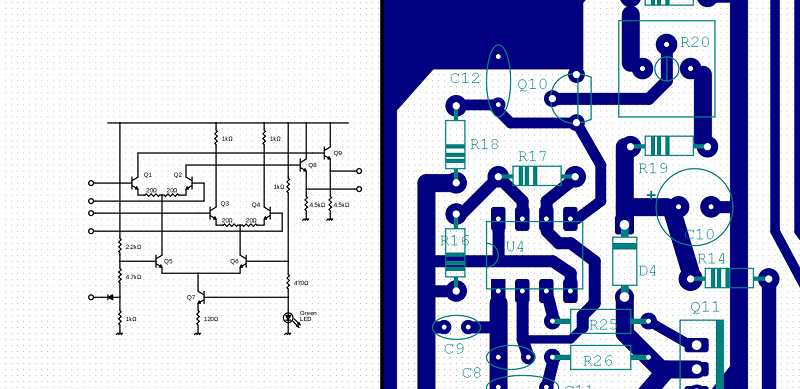
I wouldn’t be happy with the schematic shown in the image above. There are no dots showing where the lines join, and thus it is not possible to see the correct connections of the collectors of Q1-Q4.
Connection dots are perfectly visible in the program, and in the example screenshot on GitHub. Maybe they were lost in scaling the article graphic?
http://darwinne.github.io/FidoCadJ/examples/differential_amplifier.png
Um, they don’t connect to any of the crossed lines, so why should there be any dots?
Even if dots aren’t available (which would be unlikely), they’re not a necessity for drawing schematics – some style guides even recommend breaking 4-way connections into two three-way ones to make them unambiguous.
I like dots at T connections like the bases of Q3 and Q4 so that you know the tool sees that as a connection. Otherwise, finding why your traces won’t connect in the PCB means reading through the net-list. Yes, this has happened to me in the pat.
I can’t see any crossovers where they should join and have a spot, and putting spots on every T where it’s obvious they join because they have nowhere else to go is superfluous.
Assuming “superfluous” means “required by certain schematic drafting standards” then I heartily agree!
TLDR; There’s this thing, and it’s really cool, but it’s not very good. It has this feature, but I wouldn’t use it if I were you. It can even do this other thing, but not very well. Also it’s able to work with other stuff, but not the stuff we use. Anyway, it exists.
Which is a sign that this isn’t intended for regular schematic capture. It’s specifically for producing nice diagrams for documentation purposes, which is something normal EDA tools are pretty bad at.
If your documentation is in HTML then I quite like the Export to SVG option of gEDA gschem. Actually, there is no such option. I export to EPS and then use eps2svg from the `geg` package.
Does it support DXF?
[ Quote ]
Java and PCs have come a long way, so the program is fast and responsive on a modern computer.
[ /Quote ]
This has nothing to do with Java in particular.
“Modern” computers have become calculation monsters and it would be real strange if it had trouble with simple applications like this.
My own standard is KiCad, and it runs just fine on my 12 year old Dualcore.
But I have to admit, when I pull the Olinuxino A64 from github and open it in KiCad, then my PC struggles a bit with the 6 layer PCB, but even that is probably because of my cheaped out graphics card that does not do much OpenGL.
KiCad also easily exports schematics to SVG, PDF, Postscript (and more), and that should be plenty for publication.
“since it uses Java will barely run on just about any computer.”
FTFY
… as long as you’ve downloaded the right version of the Runtine Environment.
If the main strength of FidoCAD is that schematics can be easily exported to LaTeX, you do not need it. I have embedded schematics from KiCAD in LaTeX with all their full vector glory. Just plot the schematic as PDF in b/w and without the borders, and include the PDF it in KiCAD. Easy and top quality.
But it is always nice learning new things, so I will give it a try.
I know it’s been featured recently already, but everyone needs to go try LibrePCB right now!
The schematics are good, and it’s a great PCB tool. I’d hate to have to deal with two separate programs for my PCB and schematic, when I can just use one.
It’s not specifically publication focused, most of the time if I’m looking at a schematic, it was made in a PCB tool, so I’m perfectly fine with the aesthetics of decent PCB oriented schematics.
The only thing I wish it has is annotations besides the actual circuits, right in the schematics. It won’t do fancy frames or anything yet like Eagle, but it should be good enough for “Figure A” in a PDF.
No thank you.
I’m perfectly happy with KiCad, which is a very decent PCB design program and has huge high quality libraries.
And with every release some of the old “missing features” are added.
I also had a look at:
https://librepcb.org/compare/
The comparison with KiCad is simply ridiculous.
Half the statements are untrue, at least for the current state of KiCad, and others are just silly.
I also do not understand the philosophy of the designers of LibrePCB. Best I can remember from when this project was started was something like: “KiCad is not a fully polished program yet, and some things work a bit haphazardly, and we can do better”. So far just swell. But why start a new PCB design suite for that and duplicate all that effort instead of contributing to the already exising FOSS project?
I use Open Source software exclusively out of principle and I’ve seen similar things before. Instead of a few great applications for some tasks, there hare 100’s of them, most garbage, and only a few “sort of OK-ish”.
In the bigger sense I wonder why there is this failure to communicate and cooperate?
I’ve seen multiple “we like KiCad just the way it is” discussions on forums. It would be extremely hard to recreate LibrePCB’s UI in KiCad, because existing users seem to like the modularity and keyboard driven nature.
Blender is the only time I’ve seen the “Polish an existing app” strategy happen to the degree that would be needed to make KiCad an Eagle competitor.
They could fork, but as I understand it, KiCad dev isn’t that easy, everything is basically glued together separate programs, creating a completely seamless experience where everything is synced totally automatically takes some hackery.
Most thing seem to split into the “Vim style” app that gives low level control, the consumer version, and the hundreds of garbages that you mention, usually made because someone didn’t like how big something else was, and thought unused features were evil.
Merging the easy to us consumer software and the keyboard driven power user stuff for people with great memory and touch typing skill rarely ever happens, it’s like asking why we need Ubuntu when Arch and Manjaro exist. Unless you want Arch to be fixed release and have everything built around one standard batteries included setup, there’s always going to be a need for both.
“It is complementary with the big EDA electronic tools.”
With all apologies to the Unix philosophy I’d rather use just big one all-encompassing EDA tool that does everything. While I could probably sit down with any schematic capture program and figure out how to enter a schematic really getting efficient at it takes time and effort. Also, even if they had import/export options for working with every other tool you might want to use can that always be trusted? If one connection did not survive the import or export process in a large, complex design would the user notice?
I think fidocadj is not being given due credit; you can do more than just nice schematics.
Here’s a flying spaghetti monster pcb done with bezier and cubic spline based tracks:
https://hackaday.io/project/19904-noo-dleus-ex-machina-freeform-pcb-design-proto